Check patentability & draft patents in minutes with Patsnap Eureka AI!

Connection structure for improving radio-frequency performance of off chip ESD (Electro-Static Discharge) protection circuit

An ESD protection, radio frequency performance technology, applied in emergency protection circuit devices, emergency protection circuit devices for limiting overcurrent/overvoltage, circuit devices, etc. ESD protection circuit branch clamp voltage is unstable, affecting circuit impedance matching, etc., to expand the application frequency range, eliminate wave notch problems, and improve RF performance.

Inactive Publication Date: 2011-11-23
SUZHOU INNOTION TECH
View PDF2 Cites 2 Cited by
  • Summary
  • Abstract
  • Description
  • Claims
  • Application Information

AI Technical Summary

Problems solved by technology

However, since the parasitic parameters of the chip itself are connected in series with the parasitic inductance of the bonding wire, it is equivalent to a series resonant circuit connected in parallel to the signal transmission path, and the series resonant circuit will resonate at a certain frequency. The impedance is the smallest, and part of the signal will be directly transmitted to the ground through the ESD protection circuit, causing the signal to generate a wave notch
If the operating bandwidth of the RF system includes the resonant frequency of the ESD protection circuit, it will seriously affect the impedance matching of the circuit and reduce the RF performance of the circuit such as output power, gain, and efficiency.
In addition, since the bonding wire is connected in series with the branch of the ESD protection circuit, when the ESD current is discharged to the ground through the path of the ESD protection circuit, the parasitic inductance impedance of the bonding wire will cause the clamping voltage of the branch of the ESD protection circuit to be unstable

Method used


Image

  • Connection structure for improving radio-frequency performance of off chip ESD (Electro-Static Discharge) protection circuit
  • Connection structure for improving radio-frequency performance of off chip ESD (Electro-Static Discharge) protection circuit
  • Connection structure for improving radio-frequency performance of off chip ESD (Electro-Static Discharge) protection circuit

Examples


Embodiment

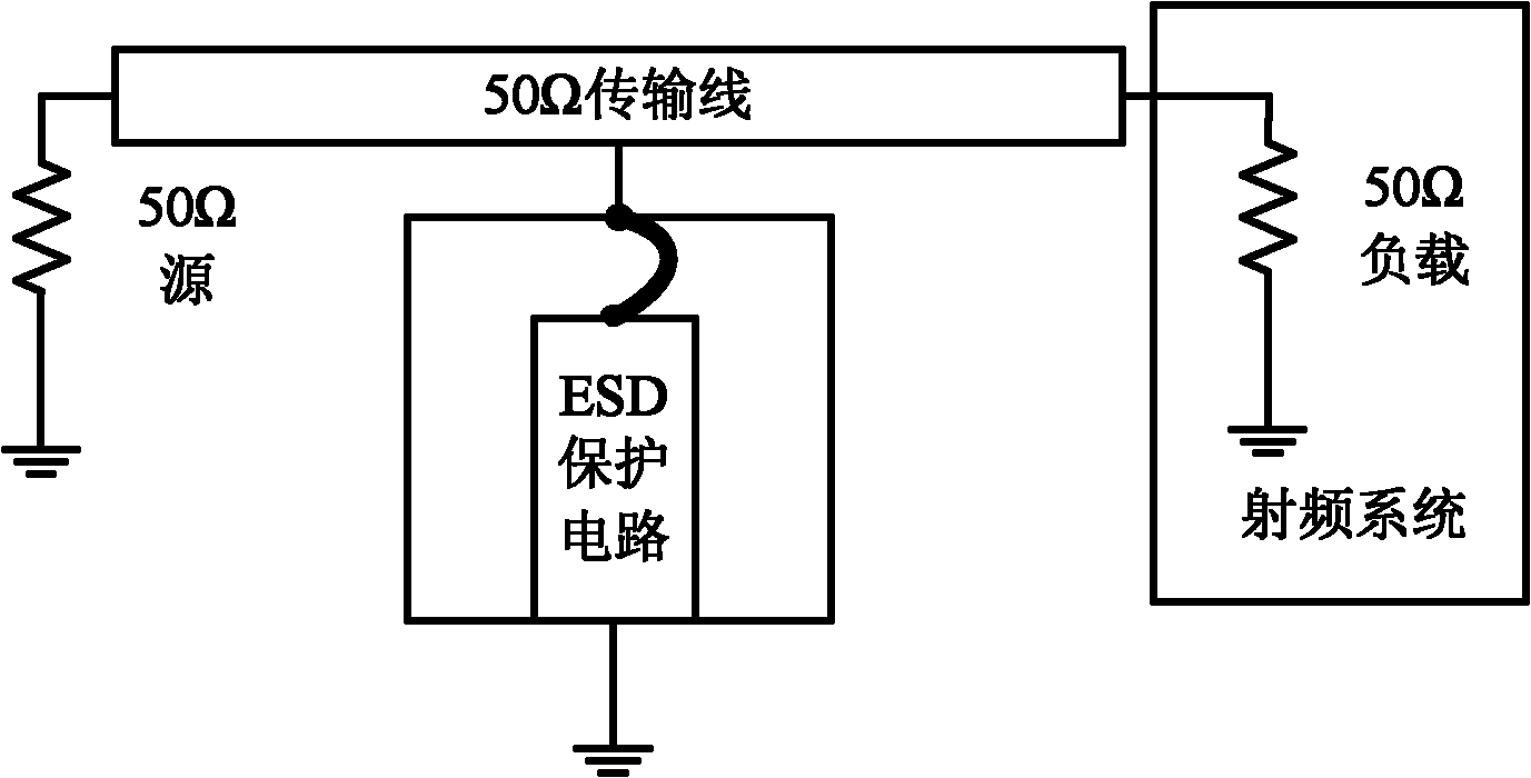
[0019] Embodiment: Any port of the system needs an ESD protection circuit to prevent electrostatic damage, mainly including a power port, a signal input port, and a signal output port. Among them, the power port does not involve signal transmission, and has relatively low requirements on the ESD protection circuit, and only the antistatic ability of the ESD protection circuit needs to be considered. The signal input port and the signal output port are the beginning and end of the signal transmission path, so not only the off-chip ESD protection circuit is required to have high anti-static ability, but also requires it to have good radio frequency performance.

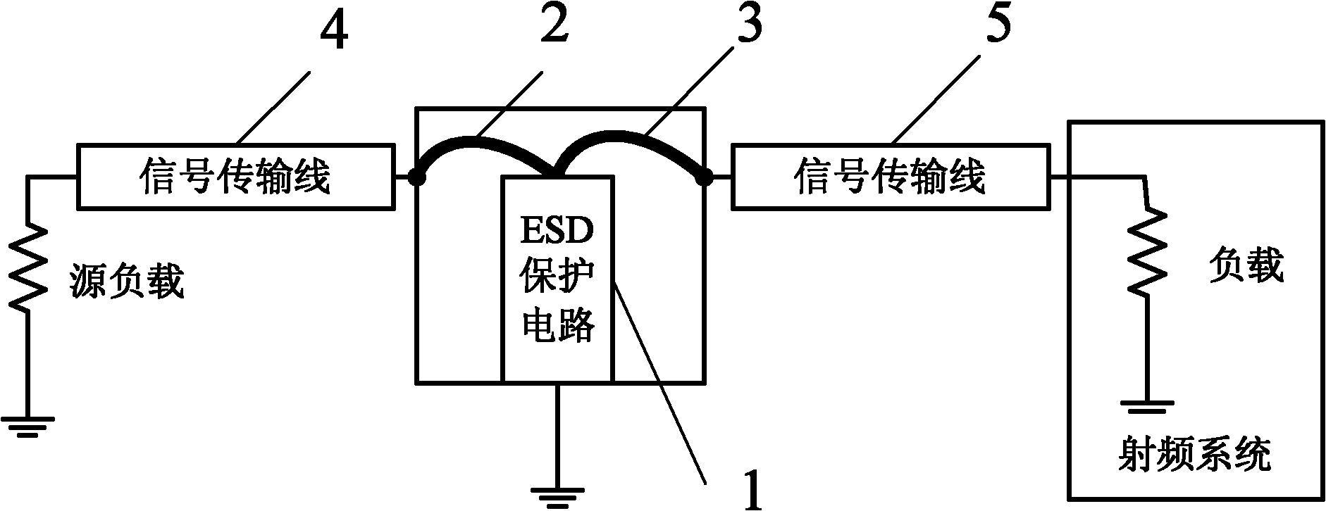
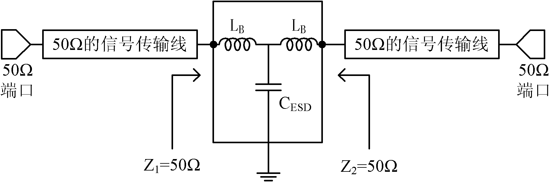
[0020] like figure 2 As shown, taking the working process of the ESD protection circuit at the input port as an example, the default radio frequency system is a 50Ω system. The improved connection structure of the off-chip ESD protection circuit is as follows: the first bonding wire 2 (bonding wire) and the second...


PUM


Abstract

The invention discloses a connection structure for improving the radio-frequency performance of an off chip ESD (Electro-Static Discharge) protection circuit. The structure comprises an off chip ESD protection circuit and a bonding line. The bonding line comprises a first bonding line and a second bonding line. The first bonding line and the second bonding line are connected end to end d in a signal transmission line in series so that the signal transmission line is separated into two sections, namely a first transmission line and a second transmission line. An input port of the off chip ESD protection circuit is connected to the junction point of the first bonding line and the second bonding line. According to the structure disclosed by the invention, on the premise of not changing self parasitic parameters of the ESD protection circuit and not reducing the anti-static electric capacity of the ESD protection circuit, the wave trapped problem resulted from the traditional ESD protection solution is eliminated; the clamping voltage stability of the ESD protection circuit is increased; the influence of the ESD protection circuit to the impedance matching of a system is improved; and the application frequency range of the off chip ESD protection circuit is expanded.

Description

technical field [0001] The invention relates to an off-chip ESD protection circuit used in the radio frequency field. Background technique [0002] Static charges exist all the time in nature. When two objects with different electrostatic potentials are close to each other or in direct contact, the transfer of static charges will occur between the two objects to form a current. This process is electrostatic discharge (ESD, Electro- Static discharge) process. The duration of ESD is very short, the typical order of magnitude is from 10ns to 100ns; the discharge current is large, ranging from 1 ampere to tens of amperes. In the entire life cycle of integrated circuits (ICs), from manufacturing, packaging, transportation, assembly and even completed IC products, they are always faced with the impact of electrostatic discharge. ESD is the most common factor in all IC failures. Take measures, ESD will cause immeasurable damage to integrated circuits or electronic products. ...

Claims


Application Information

Patent Timeline
IPC IPC(8): H02H9/04H02H9/02
Inventor 高怀杨涛张晓东王钟王寅生
Owner SUZHOU INNOTION TECH
Features
  • R&D
  • Intellectual Property
  • Life Sciences
  • Materials
  • Tech Scout
  • Unparalleled Data Quality
  • Higher Quality Content
  • 60% Fewer Hallucinations
Learn More