

A wiring structure of an induction layer
A wiring structure and sensing layer technology, which is applied in the field of wiring structure of a single-layer sensing layer, can solve the problems affecting the linearity and poor matching of the touch screen, and achieve the effect of improving linearity and good matching
- Summary
- Abstract
- Description
- Claims
- Application Information
AI Technical Summary
Problems solved by technology
Method used
Image

Examples
Embodiment Construction
[0012] The present invention will be further described below in conjunction with the accompanying drawings and embodiments.
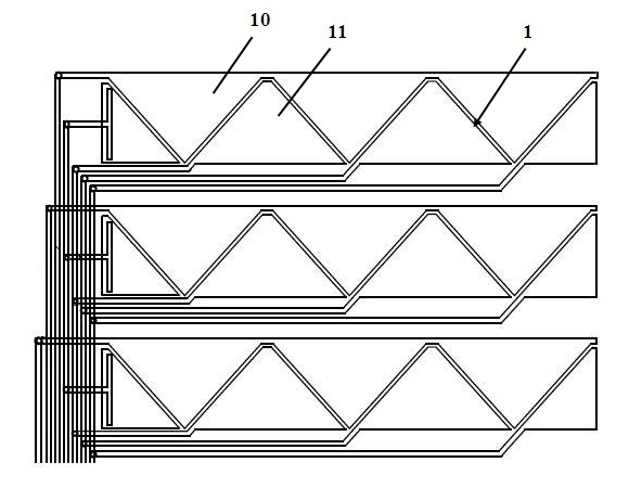
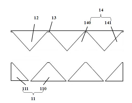
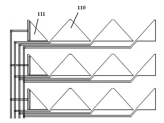
[0013] Please refer to figure 1 and figure 2 , the wiring structure of the sensing layer involved in the present invention, the sensing layer includes a plurality of touch electrode groups 1 arranged vertically, each of the touch electrode groups 1 includes a first touch electrode 10 and a plurality of second touch electrodes The electrodes 11, the first touch electrodes 10 and the second touch electrodes 11 are led out through wires. The first touch electrode 10 includes a plurality of fingers 12 , a main body 13 connecting the fingers and a plurality of notches 14 arranged laterally, and the second touch electrode 11 extends into the notches 14 . The notch 14 includes a middle notch 140 and an edge notch 141 , the edge notch 141 is located on both sides of the middle notch 140 , and the middle notch 140 is formed between two adjacent fingers ...
PUM
 Abstract
Description
Claims
Application Information