Method for manufacturing through hole pad on step structure of printed circuit board (PCB) and PCB

A technology of a ladder structure and a PCB board, which is applied to the formation of electrical connection of printed components, electrical connection of printed components, printed circuit components, etc., can solve the problems of complex manufacturing methods and high costs, and achieve simple manufacturing methods, low costs, and manufacturing methods. simple effect

Active Publication Date: 2013-01-30
NEW H3C TECH CO LTD
View PDF3 Cites 0 Cited by
  • Summary
  • Abstract
  • Description
  • Claims
  • Application Information

AI Technical Summary

Problems solved by technology

[0016] Embodiments of the present invention provide a method for manufacturing a through-hole pad at a stepped structure on a PCB and a PCB board, which solve the technical problems of complex manufacturing methods and high costs in the prior art

Method used


Image

  • Method for manufacturing through hole pad on step structure of printed circuit board (PCB) and PCB
  • Method for manufacturing through hole pad on step structure of printed circuit board (PCB) and PCB
  • Method for manufacturing through hole pad on step structure of printed circuit board (PCB) and PCB

Examples


Embodiment 1

[0051] The method for manufacturing the through-hole pad at the step structure on the PCB provided by the embodiment of the present invention at least includes the following steps:

[0052] S1. Fabrication and lamination of each inner layer;

[0053] The steps of making and laminating the inner layers in this embodiment are the same as the steps of making and laminating the inner layers in the method for making a multi-layer PCB in the prior art, and will not be repeated here. When actually manufacturing the through-hole pads on the PCB, the laminated substrate can be used directly. Of course, if the substrate is a single-layer board, the steps of making and laminating each inner layer can also be omitted.

[0054] S2, making through holes:

[0055] in such as Figure 7 A through hole 2 is processed at a preset position on the substrate 1 shown, and the opening diameter of the through hole 2 on the bottom surface 12 of the substrate 1 (the diameter refers to the inner diame...


PUM


Abstract

The embodiment of the invention provides a method for manufacturing a through hole pad on a step structure of a printed circuit board (PCB) and the PCB and relates to the technical field of PCB manufacturing. By the method, technical problems of complex manufacturing methods and quite high cost in prior art are solved. The method for manufacturing the through hole pad on the step structure of thePCB comprises the following steps of: manufacturing inner laminate layers and laminating the inner laminate layers; machining through holes at preset positions on a substrate, wherein the caliber size of an opening, on the bottom face of the substrate, of each through hole is greater than caliber size of an opening, on the top face of the substrate, of each through hole; performing electroless plating copper; electroplating copper; transferring patterns; and manufacturing a groove or a step part: forming the groove or the step part at the through hole opening on the bottom face and around theopening and the step part and keeping a part of the part with larger through hole caliber size. The PCB comprises the substrate and the step structure, wherein the through hole pad is arranged on thestep structure. The invention is applied to reduction of manufacturing cost of the printed circuit board.

Description

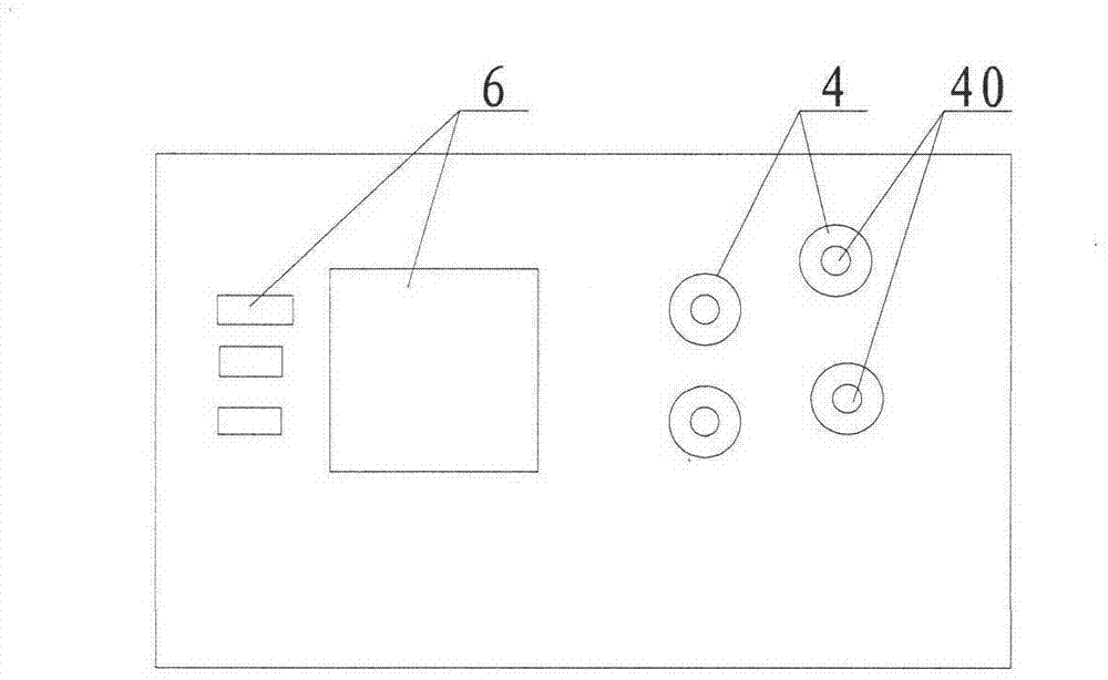
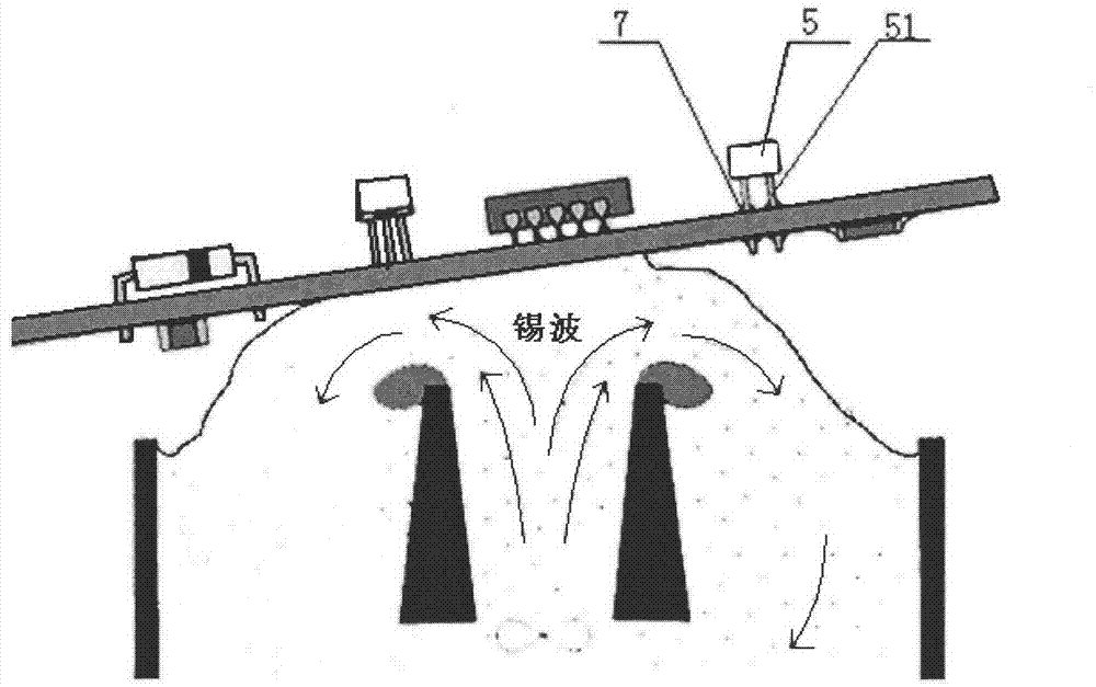
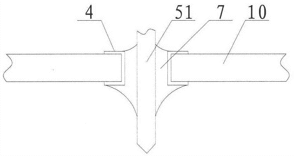
technical field [0001] The invention relates to the technical field of circuit board manufacturing, in particular to a method for manufacturing through-hole pads at stepped structures on a PCB and a PCB with corresponding through-hole pads at the stepped structures. Background technique [0002] With the rapid development of electronic technology, the demand for printed circuit boards (Printed Circuit Board, abbreviated as: circuit board or PCB board) is increasing. [0003] The pad is an important part on the circuit board, which is a solderable copper layer on the surface of the circuit board. In a conventional circuit board, the pad is used for welding various components. The pad usually includes such as figure 1 The through-hole pad (pad) 4 of the three-dimensional structure and the surface-mount pad (land) 6 of the two-dimensional structure are shown, and the surface-mount pad 6 adopts a surface mount method for welding components; Such as figure 2 As shown in the pl...

Claims


Application Information

Patent Timeline
Patent Type & Authority Patents(China)
IPC IPC(8): H05K3/40H05K1/11
Inventor 李义
Owner NEW H3C TECH CO LTD
Why Eureka
Try Eureka