Liquid crystal display panel and manufacturing method thereof

A technology for liquid crystal display panels and manufacturing methods, applied in nonlinear optics, instruments, optics, etc., can solve the problems of uneven thickness of liquid crystal display panels, poor conduction effect, mula, etc., and achieve the effect of improving the quality of picture display

Inactive Publication Date: 2012-01-25
TCL CHINA STAR OPTOELECTRONICS TECH CO LTD
View PDF3 Cites 26 Cited by
  • Summary
  • Abstract
  • Description
  • Claims
  • Application Information

AI Technical Summary

Problems solved by technology

[0007] An object of the present invention is to provide a liquid crystal display panel to solve the problem of Murla phenomenon caused by the non-uniform thickness of the liquid crystal display panel due to the separate coating of the frame glue and the conductive glue in the prior art, and the low hardness of the frame glue. The technical problem that the conductive effect is not good when the distance between the glue and the conductive glue is large

Method used


Image

  • Liquid crystal display panel and manufacturing method thereof
  • Liquid crystal display panel and manufacturing method thereof
  • Liquid crystal display panel and manufacturing method thereof

Examples


Embodiment Construction

[0033] The following descriptions of the various embodiments refer to the accompanying drawings to illustrate specific embodiments in which the present invention can be practiced.

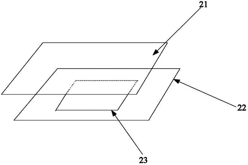
[0034] see figure 2 , figure 2 It is a structural diagram of a preferred embodiment of a liquid crystal display panel in the present invention.

[0035] The liquid crystal display panel includes a color filter substrate 21 and an array substrate 22 , and also includes a conductive sealant 23 , wherein the color filter substrate 21 and the array substrate 22 are bonded by the conductive sealant 23 .

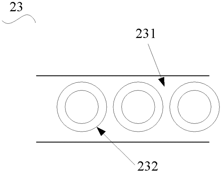
[0036] see image 3 , image 3 for figure 2 A structural diagram of a preferred embodiment of the conductive sealant 23 described in .

[0037] The conductive sealant 23 includes a sealant 231 and conductive particles 232 , wherein the conductive particles 232 are uniformly dispersed in the sealant 231 .

[0038] see Figure 4 , Figure 4 for image 3 A structural diagram of a preferred emb...


PUM

PropertyMeasurementUnit
thicknessaaaaaaaaaa

Abstract

The invention discloses a liquid crystal display panel which comprises a colored film substrate, an array substrate and a conductive frame glue, wherein the conductive frame glue is used for adhering the colored film substrate and the array substrate; the conductive frame glue contains a sealant material and conductive particles; the conductive particles are composed of organic resin ball cores and carbon nanometer tubes or graphene conductive coatings; the conductive coatings are wrapped outside the organic resin ball cores; and the conductive particles are uniformly distributed in the sealant material. The invention also discloses a manufacturing method of the liquid crystal display panel.

Description

technical field [0001] The invention relates to the field of liquid crystal display technology, in particular to a liquid crystal display panel and a manufacturing method thereof. Background technique [0002] With the continuous popularization of liquid crystal displays (Liquid Crystal Display, LCD), users have higher and higher requirements on the functions of the liquid crystal displays. [0003] LCD panel production process, please refer to figure 1 The frame glue 11 is mainly used to bond the color filter substrate 13 and the array substrate 12, and the conductive glue 14 mainly realizes the conduction function between the array substrate 12 and the color filter substrate 13, and the frame glue 11 and the conductive glue 14 are generally separated. [0004] see figure 1 After the sealant 11 is formed on the array substrate 12 , the color filter substrate 13 is pressed onto the array substrate 12 , so that the color filter substrate 13 is bonded to the array substrate ...

Claims


Application Information

Patent Timeline
Patent Type & Authority Applications(China)
IPC IPC(8): G02F1/1339G02F1/1333
CPCG02F1/1333G02F1/1339G02F1/13398
Inventor 王俊
Owner TCL CHINA STAR OPTOELECTRONICS TECH CO LTD
Why Eureka
Try Eureka