Generation method of automatic optical detecting model diagram

A technology for automatic optical detection and detection of models, which is used in material analysis, measuring devices, scientific instruments, etc. by optical means, and can solve the problem of time-consuming procedures.

Inactive Publication Date: 2012-02-08
SHENXUN COMP KUNSHAN
View PDF6 Cites 2 Cited by
  • Summary
  • Abstract
  • Description
  • Claims
  • Application Information

AI Technical Summary

Problems solved by technology

[0005] However, if there is already an automatic optical inspection program for one type of machine, and to write an optical inspection program for another similar type of machine, it is necessary to use the part position data table, and it takes a lot of time to write the program.

Method used


Image

  • Generation method of automatic optical detecting model diagram
  • Generation method of automatic optical detecting model diagram

Examples


Embodiment Construction

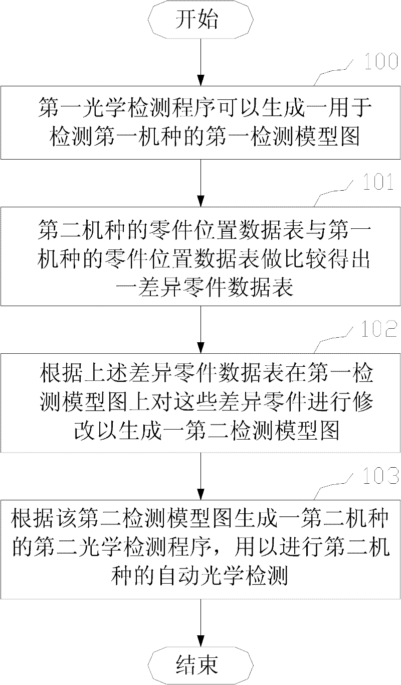
[0015] see figure 1 , figure 1 It is a method flowchart of a preferred embodiment of the method for generating an automatic optical inspection model diagram of the present invention.

[0016] The invention provides a method for generating an automatic optical inspection model diagram, which is carried out on the basis of a first optical inspection program, and the first optical inspection program can generate a first model for inspection of a first model Detection model diagram, the method is used for the generation of an optical detection model diagram of a second model similar to the first model, in this preferred embodiment, the method includes the following steps:

[0017] The first optical detection program can generate a first detection model diagram for detecting the first model (step 100);

[0018] The part position data table of the second model is compared with the part position data table of the first model to obtain a difference part data table (step 101);

[00...


PUM


Abstract

The invention provides a generation method of an automatic optical detecting model diagram, which is preformed on the basis of a first optical detecting program, wherein the first optical detecting program can generate a first detecting model diagram for detecting a first model, and the method is used for generating an optical detecting model diagram of a second model similar to the first model. The method comprises the steps: generating the first detecting model diagram for detecting the first model by the first optical detection program; comparing a part position data table of the second model with a part position data table of the first model to obtain a different part data table; modifying the different parts on the first detecting model diagram according to the different part data table to generate a second detecting model diagram; and generating a second optical detecting program of the second model according to the second detecting model diagram to automatically and optically detect the second model. Therefore, an optical detecting program programming time of the second model is reduced.

Description

【Technical field】 [0001] The invention provides a method for generating an automatic optical inspection model diagram, in particular a method for generating an automatic optical inspection model diagram for a printed circuit board. 【Background technique】 [0002] PCB (Printed Circuie Board) is the abbreviation of Printed Circuit Board, and SMT is Surface Mount Technology (Surface Mount Technology) (abbreviation of Surface Mounted Technology). Automated Optical Inspection (AOI, Automated Optical Inspection) uses high-speed and high-precision visual processing technology to automatically detect various mounting errors and soldering defects on the PCB. The range of PCB boards can range from fine-pitch high-density boards to low-density large-size boards, and online inspection solutions can be provided to improve production efficiency and welding quality. [0003] Find and eliminate errors early in the assembly process for good process control by using AOI as a defect reduction...

Claims


Application Information

Patent Timeline
Patent Type & Authority Applications(China)
IPC IPC(8): G01N21/956
Inventor 曹春龙
Owner SHENXUN COMP KUNSHAN
Why Eureka
Try Eureka