A device including a back side illuminated image sensor and a manufacture method of the image sensor

A technology of image sensing and manufacturing method, which is applied to electrical components, radiation control devices, electrical solid devices, etc., can solve the problems of crosstalk interference, insufficient isolation, and a large number of occurrences, and achieve the effect of reducing crosstalk interference

Active Publication Date: 2012-02-08
TAIWAN SEMICON MFG CO LTD
View PDF3 Cites 16 Cited by
  • Summary
  • Abstract
  • Description
  • Claims
  • Application Information

AI Technical Summary

Problems solved by technology

[0003] A back side illuminated (BSI) sensor is one type of image sensor. When the size of the transistor element shrinks with each technology generation, the current BSI image sensor suffers from Cross-talk and blooming problems that can be caused by insufficient isolation between adjacent pixels in BSI image sensors
[0004] Therefore, even though current methods of manufacturing BSI image sensing elements are generally adequate for the intended purpose, these methods are not fully compliant in every respect.

Method used


Image

  • A device including a back side illuminated image sensor and a manufacture method of the image sensor
  • A device including a back side illuminated image sensor and a manufacture method of the image sensor
  • A device including a back side illuminated image sensor and a manufacture method of the image sensor

Examples


Embodiment Construction

[0031] The following disclosure provides many different embodiments or examples for implementing different features of the present invention. The specific examples of elements and arrangements described below are used to simplify the disclosure, which are for illustration only, and are not intended to limit the disclosure. In addition, in the following description, a first feature is formed on or on a second feature may include embodiments in which the first and second features are in direct contact, and may also include an additional feature formed between the first and second features For example, the first and second features may not be in direct contact. Various features can be arbitrarily drawn in different sizes to achieve the purpose of conciseness and clarity.

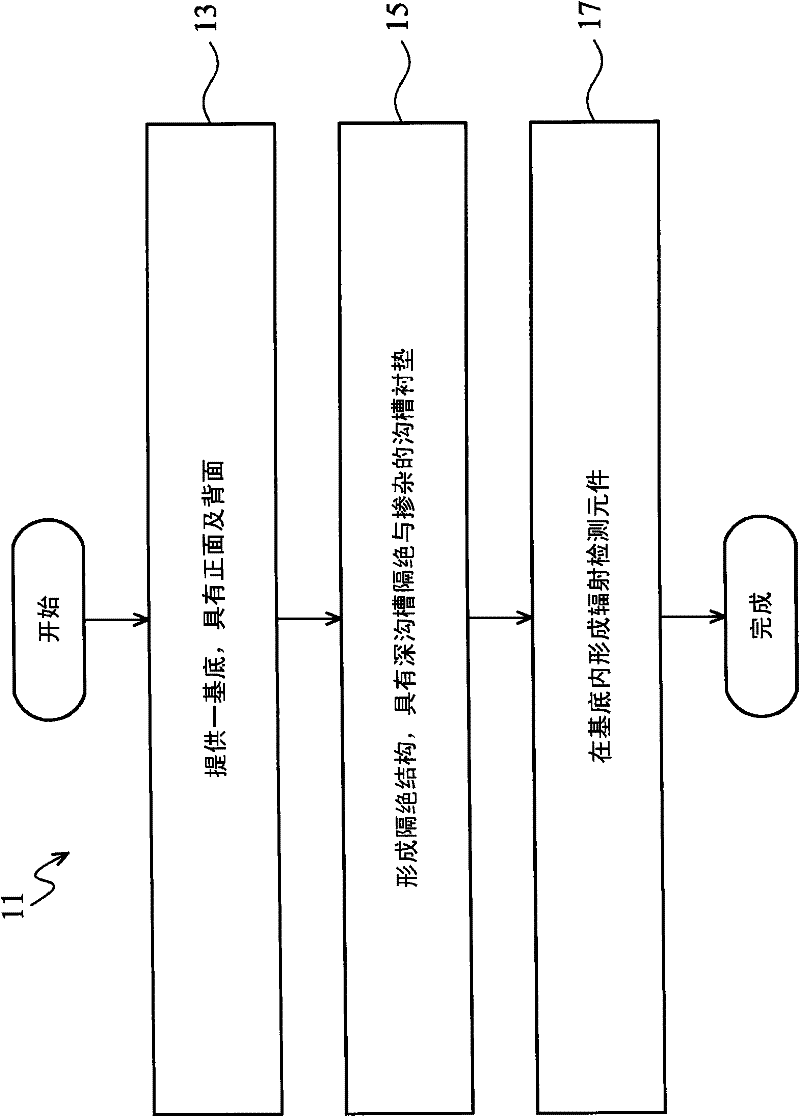
[0032] figure 1 A flowchart illustrating a method 11 of fabricating a backside illuminated (BSI) image sensing device in accordance with various concepts disclosed herein. refer to figure 1 , method 11 begin...


PUM


Abstract

Provided are a device including a back side illuminated image sensor and a manufacture method of the image sensor. The image sensor device includes a substrate having a front side and a back side opposite the front side. The image sensor also includes a radiation-detection device that is formed in the substrate. The radiation-detection device is operable to detect a radiation wave that enters thesubstrate through the back side. The image sensor further includes a deep trench isolation feature that is disposed adjacent to the radiation-detection device. The image sensor device further includes a doped layer that at least partially surrounds the deep trench isolation feature in a conformal manner. The image sensor provided by the invention is free from cross-talk.

Description

technical field [0001] The invention relates to an image sensing element, in particular to a back-illuminated image sensing element and a manufacturing method thereof. Background technique [0002] The semiconductor image sensor is used to sense light, complementary metal-oxide semiconductor (CMOS) image sensors (CIS for short) and charge-coupled device (CCD for short) Sensors are widely used in a variety of applications, such as digital still camera or mobile phone camera applications. These elements utilize pixel arrays in the substrate, including photodiodes (photodiodes) and transistors, It absorbs the radiation projected towards the substrate and converts the sensed radiation into an electronic signal. [0003] A back side illuminated (BSI) sensor is one type of image sensor. When the size of the transistor element shrinks with each technology generation, the current BSI image sensor suffers from Cross-talk and blooming problems may be caused by insufficient isolation...

Claims


Application Information

Patent Timeline
Patent Type & Authority Applications(China)
IPC IPC(8): H01L27/146H01L31/0352
CPCH01L27/1464H01L27/14643H01L27/14689
Inventor 陈思莹庄俊杰刘人诚杨敦年
Owner TAIWAN SEMICON MFG CO LTD
Why Eureka
Try Eureka