A wafer level chip scale package and a manufacturing method thereof

A technology of grain size and packaging structure, applied in the direction of microstructure technology, microstructure devices, manufacturing microstructure devices, etc., can solve problems such as chip winding, increase in component thermal resistance, and decrease in thermal characteristics

Pending Publication Date: 2019-08-02
DIALOG SEMICON UK
View PDF2 Cites 0 Cited by
  • Summary
  • Abstract
  • Description
  • Claims
  • Application Information

AI Technical Summary

Problems solved by technology

Under the condition of this thickness, there is a high probability that there will be a problem of chip winding when the assembly process is in progress
And this is why most component suppliers limit the density of the redistribution layer to only 75% o

Method used


Image

  • A wafer level chip scale package and a manufacturing method thereof
  • A wafer level chip scale package and a manufacturing method thereof
  • A wafer level chip scale package and a manufacturing method thereof

Examples


Embodiment Construction

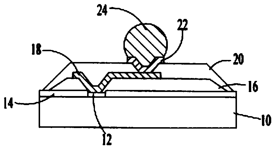
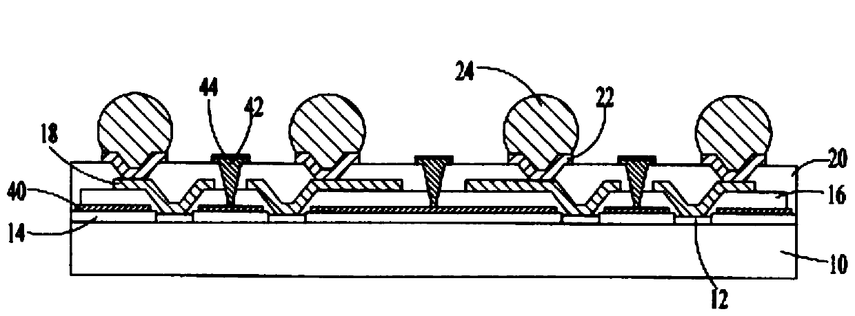
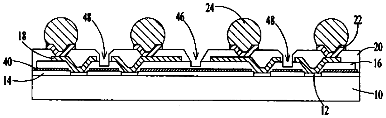
[0039] The present invention provides a method for making a wafer-level die-scale package and its package structure, which uses metal / copper plating isolation barriers and / or trench / notch air gaps to prevent crosstalk interference between adjacent signals , leakage current, and copper migration are reduced. Compared with the existing grain size packaging, the packaging structure and manufacturing process provided by the present invention can also greatly improve the thermal conductivity of the packaging structure.

[0040] The wafer-level grain size packaging technology provided by the present invention further includes the following advantages:

[0041] Compared with the traditional wafer-level die-scale package structure, it has similar appearance variables.

[0042] Compared with the traditional wafer-level grain size packaging structure, it has a similar manufacturing process.

[0043] In the future, without considering the cross-coupling, the process specifications with...


PUM

PropertyMeasurementUnit
Widthaaaaaaaaaa
Heightaaaaaaaaaa
Thicknessaaaaaaaaaa

Abstract

A wafer level chip scale package and a manufacturing method thereof are disclosed. The wafer level chip scale package comprises a plurality of redistribution layer (RDL) circuits connected to a silicon wafer through openings of a first polymer layer, with the openings penetrating the first polymer layer to connect the redistribution layer circuits to metal pads on a top surface of the silicon wafer; a plurality of underbump metal (UBM) layers each of which is in contact with one of the plurality of RDL circuits through openings in a second polymer layer over the first polymer layer; a plurality of solder bumps which lie on each UBM layer; a metal plating layer which lies under the first polymer layer and does not contact any of the plurality of RDL circuits; and at least one separator which lies between at least two of the plurality of RDL traces. The separator is a metal fencing between the two neighboring RDL circuits or an air gap between the two neighboring RDL circuits.

Description

technical field [0001] The present invention relates to a wafer packaging technology, and in particular to reduce crosstalk interference, copper migration, and leakage current in wafer-level die size packaging. Background technique [0002] Based on the fact that semiconductor chips, wafers, or integrated circuits may encounter physical damage when connected to the applied printed circuit board, or during user operation, in order to achieve the purpose of protecting these circuits, these integrated Proper packaging of the circuit is necessary. For example, several common package types currently on the market include: lead frame packages, ball grid array packages, and chip scale packages, such as: wafer-level Grain size package (wafer level chip scale package) and so on. [0003] Among them, the wafer-level chip size package (WLCSP) has the smallest form factor, because its package size is at the same level as the wafer size, and it has good electrical, structural, and ther...

Claims


Application Information

Patent Timeline
IPC IPC(8): H01L23/488H01L23/522H01L21/48
CPCH01L23/488H01L23/522H01L21/4814H01L2924/3511H01L2924/10253H01L2224/11334H01L2224/13101H01L24/05H01L24/11H01L24/13H01L2224/0401H01L2224/13111H01L2924/14H01L23/525H01L2224/05558H01L24/06H01L24/03H01L2224/0346H01L2224/0345H01L2224/0347H01L2224/05012H01L2224/023H01L2924/00H01L2924/00012H01L2924/014H01L2924/00014H01L2924/01047H01L2924/01029H01L2924/0001H01L23/3128H01L23/3114B81C1/00896H01L24/94H01L2224/73204H01L23/49816H01L29/0649H01L2224/32225H01L21/568
Inventor 哈皮·莫汀·穆罕默德拉吉·沙亚·安德拉
Owner DIALOG SEMICON UK
Why Eureka
Try Eureka