Rear electrode structure for use in photovoltaic device such as CIGS/CIS photovoltaic device and method of making same

Inactive Publication Date: 2009-01-22
GUARDIAN GLASS LLC
View PDF17 Cites 105 Cited by
  • Summary
  • Abstract
  • Description
  • Claims
  • Application Information

AI Technical Summary

Benefits of technology

[0015]The textured interior surface of the rear electrode is advantageous in several example respects. The textured surface of the rear electrode improves adhesion between the rear electrode and the semiconductor film. Moreover, the textured surface of the rear electrode allows the rear electrode to act as a scattering back electrode thereby permitting it to reflect incident light more effectively and efficiently into the light absorption semiconductor film. This can allow one of both of: improved efficiency of the photovoltaic device, and/or reduced thickness of the light absorption semiconductor film without sacrificing solar efficiency. In certain example embodiments, after the rear electrode has been formed on the rear glass substrate, the major surface of the rear electrode to be close

Problems solved by technology

However, Mo rear electrodes suffer from the pr

Method used


Image

  • Rear electrode structure for use in photovoltaic device such as CIGS/CIS photovoltaic device and method of making same
  • Rear electrode structure for use in photovoltaic device such as CIGS/CIS photovoltaic device and method of making same
  • Rear electrode structure for use in photovoltaic device such as CIGS/CIS photovoltaic device and method of making same

Examples


Embodiment Construction

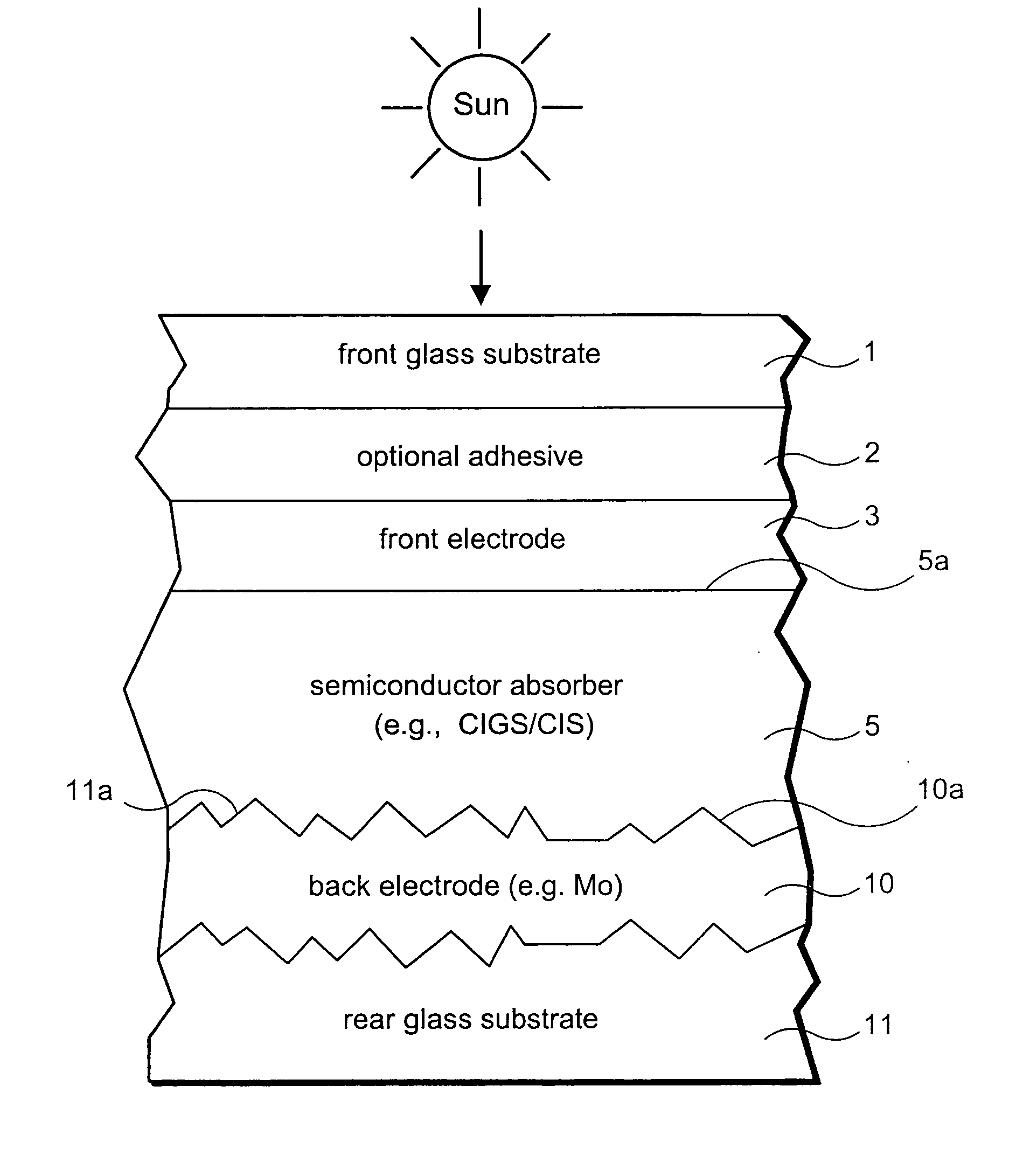
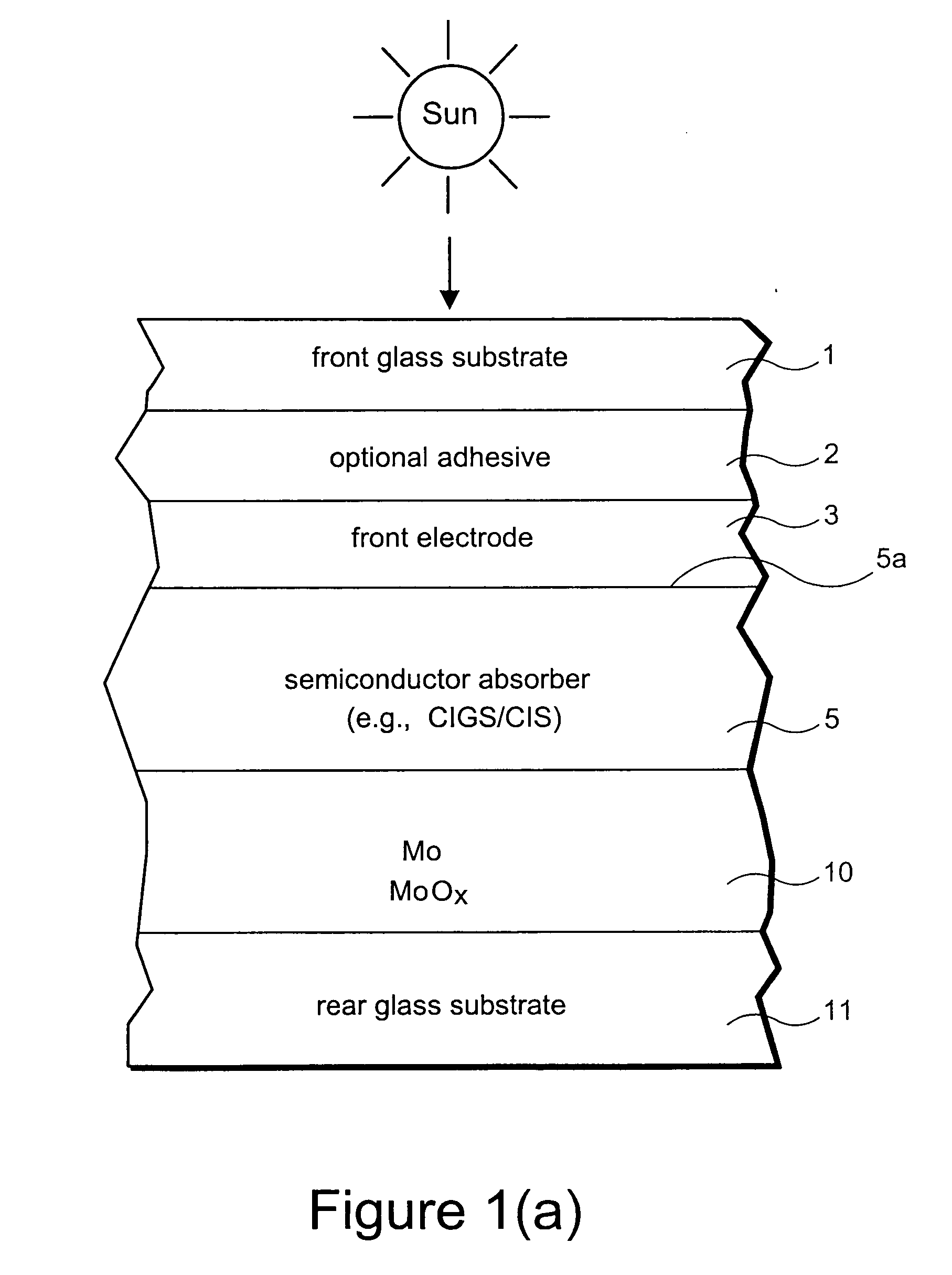
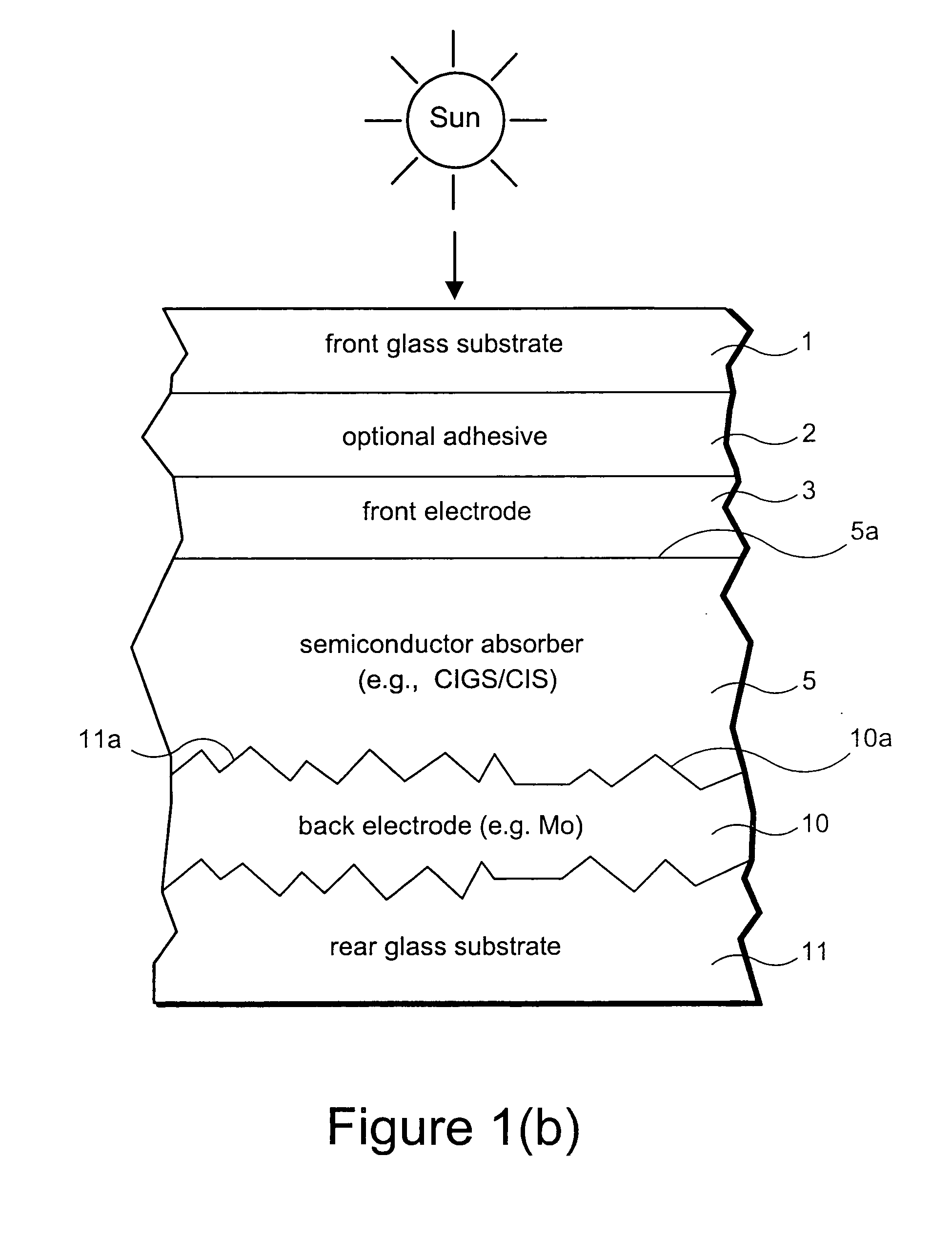
[0029]Referring now more particularly to the figures in which like reference numerals refer to like parts / layers in the several views.

[0030]Photovoltaic devices such as solar cells convert solar radiation into usable electrical energy. The energy conversion occurs typically as the result of the photovoltaic effect. Solar radiation (e.g., sunlight) impinging on a photovoltaic device and absorbed by an active region of semiconductor material (e.g., a semiconductor film including one or more semiconductor layers such as a-Si, CIS, CIGS or the like, the semiconductor sometimes being called an absorbing layer or film) generates electron-hole pairs in the active region. The electrons and holes may be separated by an electric field of a junction in the photovoltaic device. The separation of the electrons and holes by the junction results in the generation of an electric current and voltage. In certain example embodiments, the electrons flow toward the region of the semiconductor material h...


PUM

PropertyMeasurementUnit
Fractionaaaaaaaaaa
Fractionaaaaaaaaaa
Electrical conductoraaaaaaaaaa

Abstract

A photovoltaic device including a rear electrode which may also function as a rear reflector. In certain example embodiments of this invention, the rear electrode includes a metallic based reflective film that is oxidation graded, so as to be more oxided closer to a rear substrate (e.g., glass substrate) supporting the electrode than at a location further from the rear substrate. In other words, the rear electrode is oxidation graded so as to be less oxided closer to a semiconductor absorber of the photovoltaic device than at a location further from the semiconductor absorber in certain example embodiments. In certain example embodiments, the interior surface of the rear substrate may optionally be textured so that the rear electrode deposited thereon is also textured so as to provide desirable electrical and reflective characteristics. In certain example embodiments, the rear electrode may be of or include Mo and/or MoOx, and may be sputter-deposited using a combination of MoOx and Mo sputtering targets.

Description

[0001]This is a continuation-in-part (CIP) of U.S. patent application Ser. Nos. 11 / 892,161, filed Aug. 20, 2007, and 11 / 808,764, filed Jun. 12, 2007, the entire disclosures of which are hereby incorporated herein by reference.[0002]This invention relates to a rear electrode for use in a photovoltaic device or the like, and methods of making the same. The rear (or back) electrode may also function as a rear (or back) reflector in certain example instances. In certain example embodiments of this invention, the rear electrode comprises a metallic based reflective film that is oxidation graded, so as to be more oxided closer to a rear substrate (e.g., glass substrate) supporting the electrode than at a location further from the rear substrate. In other words, the rear electrode is oxidation graded so as to be less oxided closer to a semiconductor absorber of the photovoltaic device than at a location further from the semiconductor absorber. In certain example embodiments, there is provi...

Claims


Application Information

Patent Timeline
IPC IPC(8): H01L31/00C23C14/00
CPCH01L31/022425H01L31/0236Y02E10/541H01L31/0392H01L31/0749H01L31/0322H01L31/03923H01L31/02366Y02P70/50
Inventor KRASNOV, ALEXEYDEN BOER, WILLEMTHOMSEN, SCOTT V.BOYER, JR., LEONARD L.
Owner GUARDIAN GLASS LLC
Why Eureka
Try Eureka