Flat-plate X ray detector and preparation method thereof
An X-ray and detector technology, which is applied in the field of exposure control of X-ray detectors and flat-panel X-ray detectors, can solve problems affecting the image quality of flat-panel X-ray detectors and the reduction of the opening ratio of X-ray detectors.
- Summary
- Abstract
- Description
- Claims
- Application Information
AI Technical Summary
Problems solved by technology
Method used
Image
Examples
Embodiment 1
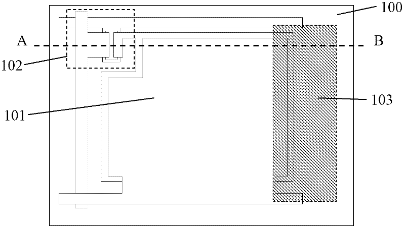
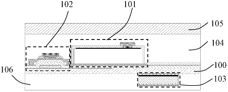
[0043] The detecting element in this embodiment adopts PIN photodiode, see figure 1 , is a schematic top view of the flat-panel X-ray detector in this embodiment. The upper surface of the glass substrate 100 includes a detection pixel, and the detection pixel includes a PIN photodiode 101, a TFT 102 and a light-transmitting element-free area. The lower surface of the glass substrate includes a detection element 103 , and the area covered by the detection element 103 includes a part of the lower surface of the upper surface photoelectric conversion element PIN photodiode covering the substrate and a lower surface of the substrate in an element-free area. In order to make the schematic representation of this embodiment more clearly, see figure 2 ,yes figure 1 In the cross-sectional view along the line AB, the photoelectric conversion element PIN photodiode 101 and the control element TFT102 are located on the upper surface of the substrate 100, and the upper surface of the detec...
Embodiment 2
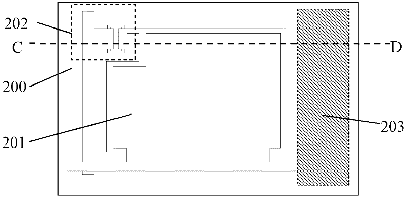
[0047] The detecting element in this embodiment adopts PIN photodiode, see image 3 , is a schematic top view of the flat-panel X-ray detector in this embodiment, the upper surface of the glass substrate 200 includes a detection pixel, the detection pixel includes a PIN photodiode 201, TFT 202 and a transparent component-free area, and the lower surface of the glass substrate includes a detection pixel Component 203, the detection component 203 covers only the lower surface of the substrate in the component-free area of the detection pixel. In order to make the schematic representation of this embodiment more clearly, see Figure 4 ,yes image 3 In the cross-sectional view along the line CD, the photoelectric conversion element PIN photodiode 201 and the control element TFT202 are located on the upper surface of the substrate 200, and the upper surface of the detector is covered by a dielectric layer 204, and above the dielectric layer is a scintillator that converts X-rays...
Embodiment 3
[0050] see Figure 5 , is a schematic top view of the flat-panel X-ray detector in this embodiment. The upper surface of the substrate 300 includes a plurality of detection pixels 301 (shown in dotted line boxes) for detecting X-rays, and the detection pixels include photoelectric conversion elements PIN photodiodes 302 . The control element TFT 303 and the element-free area, the detection element 304 is located on the lower surface of the substrate, and the detection element coverage area includes the lower surface of the substrate in the element-free area in the pixel 301 . In this embodiment, the upper surface of the substrate includes 9 pixels, and the lower surface of the substrate includes 1 detection element as an example. In an actual flat-panel X-ray detector, thousands of such pixels and multiple detection elements may be included. The detection element Usually distributed in a specific area in the pixel array of a flat-panel X-ray detector, such as Figure 6 L, R a...
PUM
 Abstract
Description
Claims
Application Information


