

Solid imaging device and electronic apparatus
A technology of solid-state imaging devices and components, which is applied in the direction of electric solid-state devices, semiconductor devices, radiation control devices, etc., can solve problems such as the influence of characteristics of solid-state imaging devices, achieve high image quality, and improve the effect of image quality
Active Publication Date: 2012-04-04
SONY CORP
View PDF16 Cites 13 Cited by
- Summary
- Abstract
- Description
- Claims
- Application Information
AI Technical Summary
Problems solved by technology
In addition, the subtle hot-carrier emission emitted from the transistor (which rarely causes problems in the normal circuit operation of the transistor) also has a great influence on the characteristics of the solid-state imaging device
Method used
View moreImage
Smart ImageViewing Examples

Examples
no. 1 example
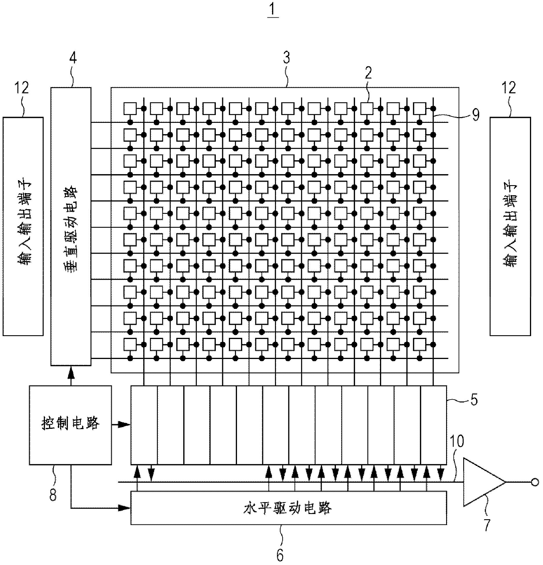
[0040] 2. First Embodiment (Structure Example of Solid-State Imaging Device)
no. 2 example
[0041] 3. Second Embodiment (Structure Example of Solid-State Imaging Device)
no. 3 example
[0042] 4. Third Embodiment (Structure Example of Solid-State Imaging Device)
Login to View More PUM
 Abstract
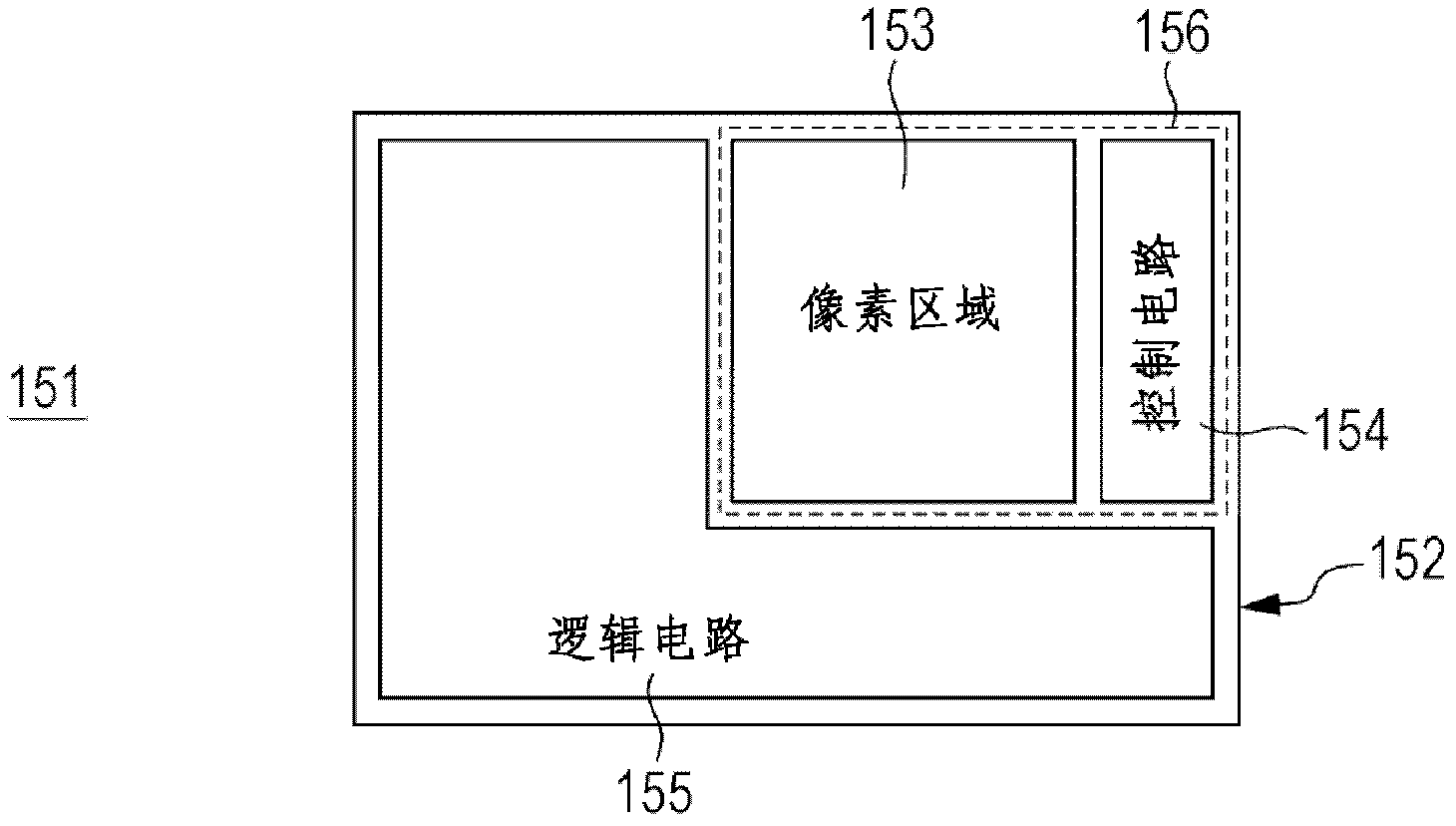
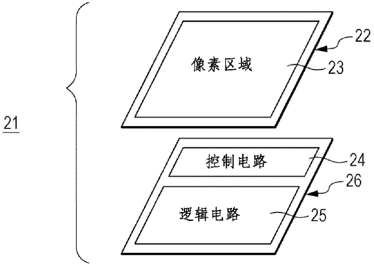
The present invention discloses a solid imaging device and an electronic apparatus, wherein the solid imaging device including: a pixel region that is formed on a light incidence side of a substrate and to which a plurality of pixels that include photoelectric conversion units is arranged; a peripheral circuit unit that is formed in a lower portion in the substrate depth direction of the pixel region and that includes an active element; and a light shielding member that is formed between the pixel region and the peripheral circuit unit and that shields the incidence of light, emitted from an active element, to the photoelectric conversion unit. The electronic apparatus comprises an optical system, a signal processing circuit and the solid imaging device. The solid imaging device and the electronic apparatus can inhibit the light outgoing from the active element to the photoelectric conversion units, thereby increasing the image quality of the solid imaging device.
Description
[0001] Cross References to Related Applications [0002] This application contains subject matter related to that disclosed in Japanese Priority Patent Application JP 2010-206890 filed in the Japan Patent Office on Sep. 15, 2010, the entire content of which is hereby incorporated by reference. technical field [0003] The present invention relates to a solid-state imaging device and an electronic device including the solid-state imaging device, such as a camera. Background technique [0004] In recent years, electronic cameras have become increasingly common, and the demand for solid-state imaging devices (image sensors), which are core components of electronic cameras, has further increased. In terms of performance, technological development is ongoing to achieve improvements in image quality and functionality. At the same time, video cameras and portable cameras, mobile phones, personal digital assistants (Personal Digital Assistant, PDA) and notebook computers have been ...
Claims
Login to View More Application Information
Patent Timeline
 Patent Type & AuthorityApplications(China)
IPC IPC(8): H04N5/335H04N5/374H01L27/146H04N5/225H04N25/00H04N23/90
CPCH01L27/14636H01L27/1464H01L27/14609H01L27/14645H04N5/369H04N5/374H01L27/14623H01L27/14603H01L27/14605H01L27/14612H01L27/1462H01L27/14621H01L27/14625H01L27/14627H01L27/14629H01L27/14643H04N23/54H04N23/55H04N25/70H04N25/76H04N25/766H04N25/77
Inventor小林正治工藤义治佐野拓也
OwnerSONY CORP