Vertical coplanar waveguide with tunable characteristic impedance, design structure and method of fabricating the same

A characteristic impedance and vertical alignment technology, applied to waveguides, waveguide devices, circuits, etc., can solve problems such as prolonging the design cycle and product launch time

Active Publication Date: 2012-04-25
格芯公司
View PDF1 Cites 0 Cited by
  • Summary
  • Abstract
  • Description
  • Claims
  • Application Information

AI Technical Summary

Problems solved by technology

Therefore, instead of modeling, most designers rely on hardware measurements of fabricated prototypes to validate chip designs, which lengthens design cycles and time-to-market

Method used


Image

  • Vertical coplanar waveguide with tunable characteristic impedance, design structure and method of fabricating the same
  • Vertical coplanar waveguide with tunable characteristic impedance, design structure and method of fabricating the same
  • Vertical coplanar waveguide with tunable characteristic impedance, design structure and method of fabricating the same

Examples


Embodiment Construction

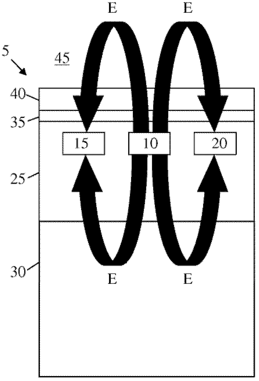
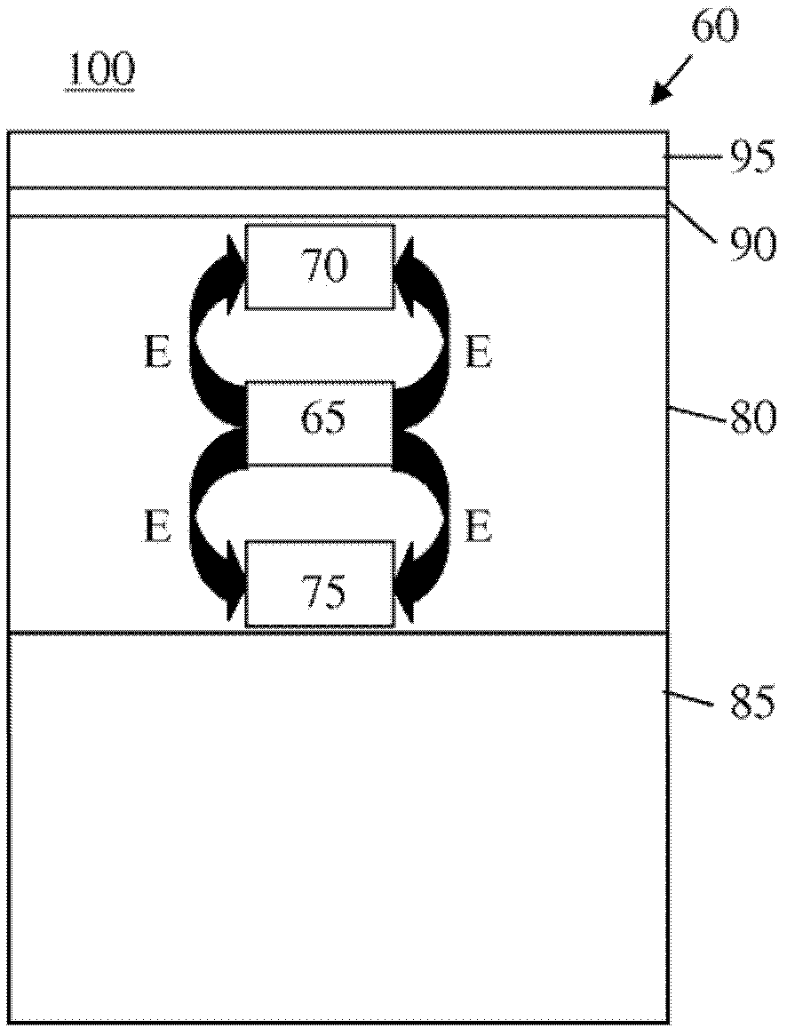
[0015] The present invention generally relates to on-chip transmission lines, and more particularly to on-chip vertical coplanar waveguides with tunable characteristic impedance, design structures and methods of manufacture thereof. In an embodiment, the on-chip transmission line includes a signal line formed in a wiring layer on the active device. The first ground line is formed in the wiring layer below the signal line and separated from the signal line by a dielectric material. The second ground line is formed in the wiring layer above the signal line, and is also separated from the signal line by a dielectric material. The signal line and the two ground lines are vertically aligned in the dielectric material, which creates a substantially symmetrical electric field for the vertical coplanar waveguide. In this way, embodiments of the present invention provide design structures that are easier to accurately model.

[0016] According to aspects of the present invention, the...


PUM

PropertyMeasurementUnit
Heightaaaaaaaaaa

Abstract

An on-chip vertical coplanar waveguide with tunable characteristic impedance, a design structure, and a method of making the same. An on-chip transmission line (60) includes a signal line (65), an upper ground line (70) spaced apart from and above the signal line, and a lower ground line (75) spaced apart from and below the signal line. The signal line, the upper ground line and the lower ground line are substantially vertically aligned in a dielectric material (80).

Description

technical field [0001] The present invention generally relates to on-chip transmission lines, and more particularly to on-chip vertical coplanar waveguides with tunable characteristic impedance, design structures and fabrication methods thereof. Background technique [0002] The performance of on-chip interconnects (eg, on-chip transmission lines) is an important factor affecting overall chip performance. On-chip transmission lines are typically modeled before production begins to minimize design time. Due to the importance of on-chip transmission lines to overall chip performance, accurate models of on-chip transmission lines are required when evaluating high-performance designs. Any errors in the transmission line model can lead to inaccurate estimates of the characteristic impedance and / or attenuation associated with the on-chip transmission line. Chips produced based on incorrect modeling may not perform in the manner required by design specifications, and thus be an i...

Claims


Application Information

Patent Timeline
IPC IPC(8): H01P3/00H01P3/18
CPCH01P3/003H01P3/085
Inventor E.米娜王国安
Owner 格芯公司
Why Eureka
Try Eureka