Multi-metal coplanar waveguide

a coplanar waveguide and multi-metal technology, applied in waveguides, multiple-port networks, electrical appliances, etc., can solve problems such as methods that are unlike, and achieve the effects of enhancing the performance of millimeter wave cmos ic, reducing the attenuation of cpw, and increasing fidelity

Inactive Publication Date: 2007-10-18
ELECTRONICS & TELECOMM RES INST
View PDF9 Cites 60 Cited by
  • Summary
  • Abstract
  • Description
  • Claims
  • Application Information

AI Technical Summary

Benefits of technology

[0009]The present invention is directed to providing various structures of ground lines applicable to a CPW using multi-layer interconnection CMOS technology, the structures increasing fidelity and reducing attenuation of a CPW to enhance performance of a millimeter wave CMOS IC.
[0010]The present invention is also directed to a CPW that is capable of minimizing CPW loss and improving fidelity by maximizing an area of electromagnetic wave propagation using a method of decreasing widths of intermediate metal layers from the ground line of the uppermost layer to a lowermost layer, a method of increasing widths of intermediate metal layers from an intermediate metal layer disposed just below the ground line of the uppermost layer to the lowermost layer, a method of using intermediate metal layers having a narrow width compared to the ground line of the uppermost layer, or a method of connecting intermediate metal layers composed of wide and narrow layers in turn, which is narrower than the ground line of the uppermost layer, to connect the ground lines of the lowermost and uppermost layers. These methods are unlike a conventional method of connecting ground lines of lowermost and uppermost layers using intermediate metal layers having the same width and via holes.
[0011]The present invention is also directed to a CPW that is capable of minimizing CPW loss and maximizing a slow wave effect by forming a patterned ground line in an intermediate metal layer as well as forming a slotted ground line or a patterned ground line in a lowermost metal layer to reduce loss caused by an image current, thereby improving performance of an ultra-high frequency circuit and miniaturizing the circuit.

Problems solved by technology

These methods are unlike a conventional method of connecting ground lines of lowermost and uppermost layers using intermediate metal layers having the same width and via holes.

Method used


Image

  • Multi-metal coplanar waveguide
  • Multi-metal coplanar waveguide
  • Multi-metal coplanar waveguide

Examples


Embodiment Construction

[0027]Hereinafter, exemplary embodiments according to the present invention will be described in detail with reference to accompanying drawings. The following embodiments will be provided to those skilled in the art to fully understand the present invention.

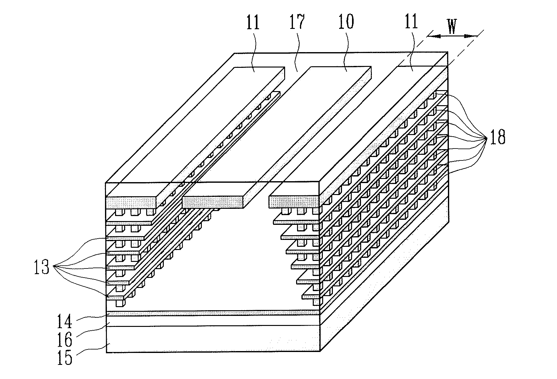
[0028]FIG. 1 is a cross-sectional view of a conventional coplanar waveguide (CPW) using multi-layer interconnection CMOS technology.

[0029]As shown in FIG. 1, in the conventional CPW using multi-layer interconnection CMOS technology, an uppermost metal layer of an 8-level metal layer forms a signal line 100 and a ground line 101, and a lowermost metal layer 104 forms a shield layer. The uppermost and lowermost metal layers are grounded using intermediate metal layers 103 and via holes 108. Each of the intermediate metal layers 103 has the same width as the ground line 101 of the uppermost metal layer, and is connected to the lowermost metal layer 104. Each metal layer is separately disposed over a silicon substrate 105 and has int...


PUM


Abstract

A coplanar waveguide CPW using multi-layer interconnection CMOS technology is provided. In the CPW including an interlayer insulator disposed on a substrate, metal multilayers disposed on the interlayer insulator, and a ground line-a signal line-a ground line formed of an uppermost metal layer, when a ground line of a lowermost layer is connected to the ground line of the uppermost layer, intermediate metal layers are designed to gradually increase or decrease in width, or to be uneven so as to maximize an area where an ultra-high frequency spreads, thereby minimizing CPW loss and maximizing a slow wave effect. As a result, it is possible to improve performance of an ultra-high frequency circuit and miniaturize the circuit.

Description

CROSS-REFERENCE TO RELATED APPLICATION[0001]This application claims priority to and the benefit of Korean Patent Application No. 2006-0033587, filed Apr. 13, 2006, the disclosure of which is incorporated herein by reference in its entirety.BACKGROUND[0002]1. Field of the Invention[0003]The present invention relates to a multi-metal coplanar waveguide (CPW) which can enhance fidelity and minimize loss of a CPW by designing a ground line in various shapes when a CPW transmission line is designed using multi-layer interconnection CMOS technology in order to apply to the design of a CMOS IC operating at ultra high frequency.[0004]2. Discussion of Related Art[0005]In design of a conventional CPW using multi-layer interconnection CMOS technology, a method of designing an uppermost metal layer to have a ground-signal-ground line structure has been used. In addition, a method of shielding the CPW by inserting a ground line below the CPW as a lowermost metal layer in order to reduce a CPW lo...

Claims


Application Information

Patent Timeline
Patent Type & Authority Applications(United States)
IPC IPC(8): H01P3/08
CPCH01P3/003H01L21/3205
Inventor KIM, CHEON SOOKWAK, MYUNG SHINKIM, SEONG DOPARK, MUN YANGYU, HYUN KYUJUNG, HEE BUM
Owner ELECTRONICS & TELECOMM RES INST
Why Eureka
Try Eureka