Multibeam Arrays of Optoelectronic Devices for High Frequency Operation

a technology of optoelectronic devices and arrays, applied in semiconductor laser optical devices, lasers, semiconductor lasers, etc., can solve the problems of increasing heat generation, vcsel arrays that provide both high frequency modulation and high power, and common degradation of edge-emitting lasers

Active Publication Date: 2010-12-02
LUMENTUM OPERATIONS LLC
View PDF7 Cites 60 Cited by
  • Summary
  • Abstract
  • Description
  • Claims
  • Application Information

AI Technical Summary

Benefits of technology

[0002]An embodiment relates to semiconductor devices and, more particularly, to multibeam arrays of ...

Problems solved by technology

However, degradation of these edge-emitting lasers is common, primarily as a result of Catastrophic Optical Damage (COD) that occurs due to high optical power density at the exposed emission facet.
However, with existing VCSEL designs, as the area of the array grows the frequency response has been penalized by heating complexities arising from the multi-ele...

Method used


Image

  • Multibeam Arrays of Optoelectronic Devices for High Frequency Operation
  • Multibeam Arrays of Optoelectronic Devices for High Frequency Operation
  • Multibeam Arrays of Optoelectronic Devices for High Frequency Operation

Examples


Embodiment Construction

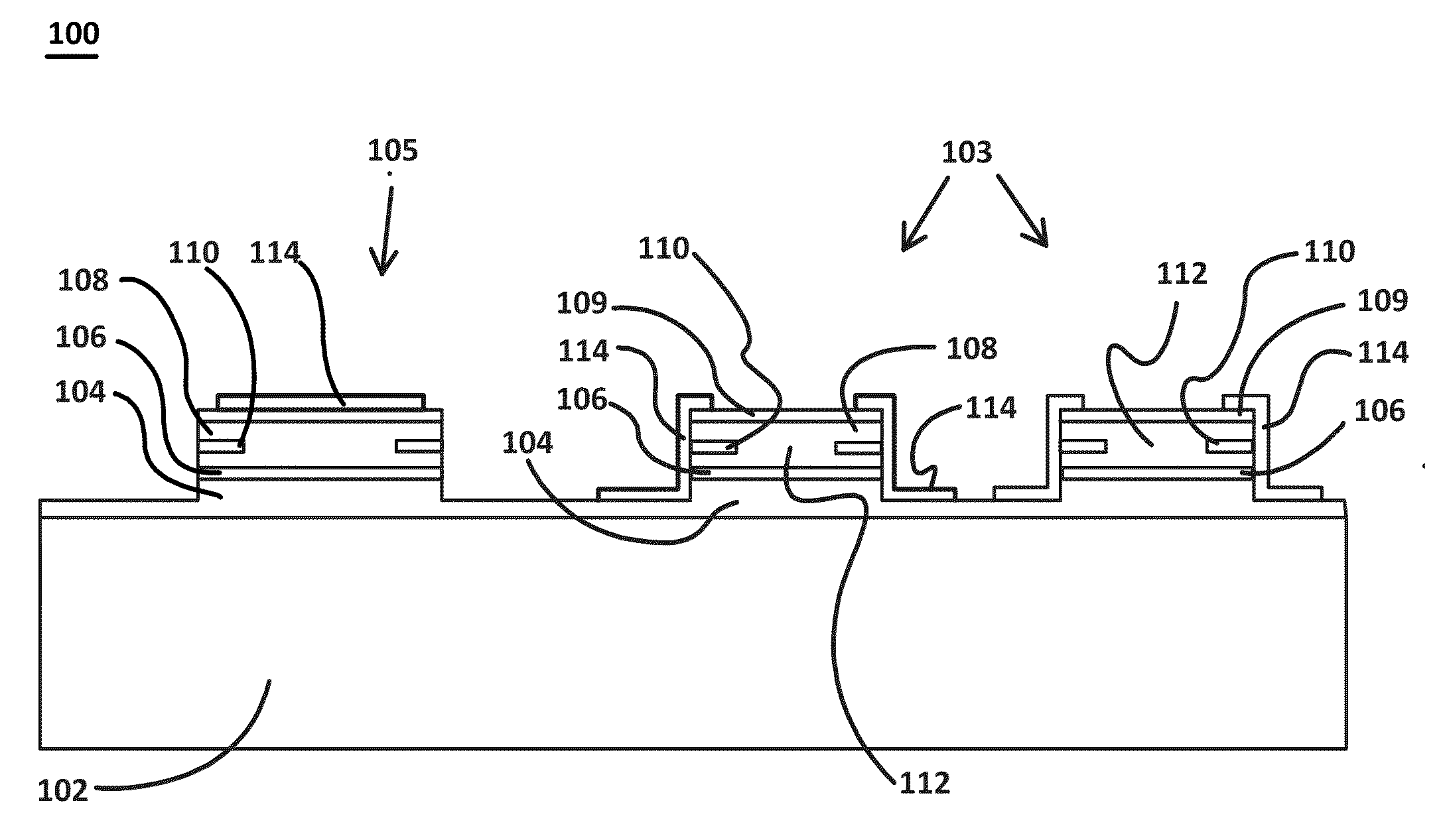
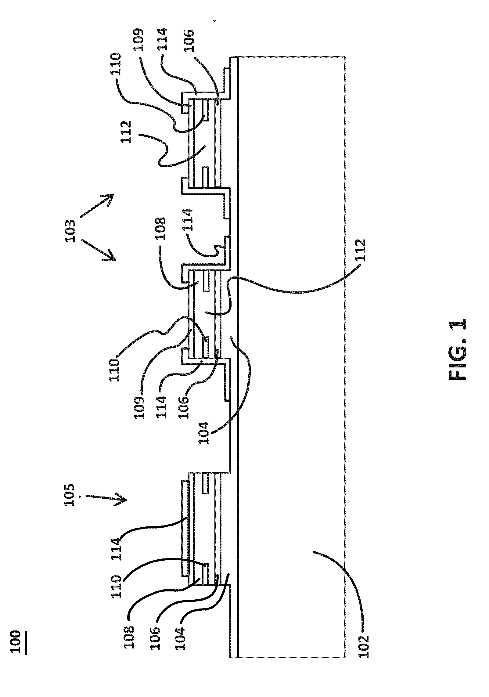
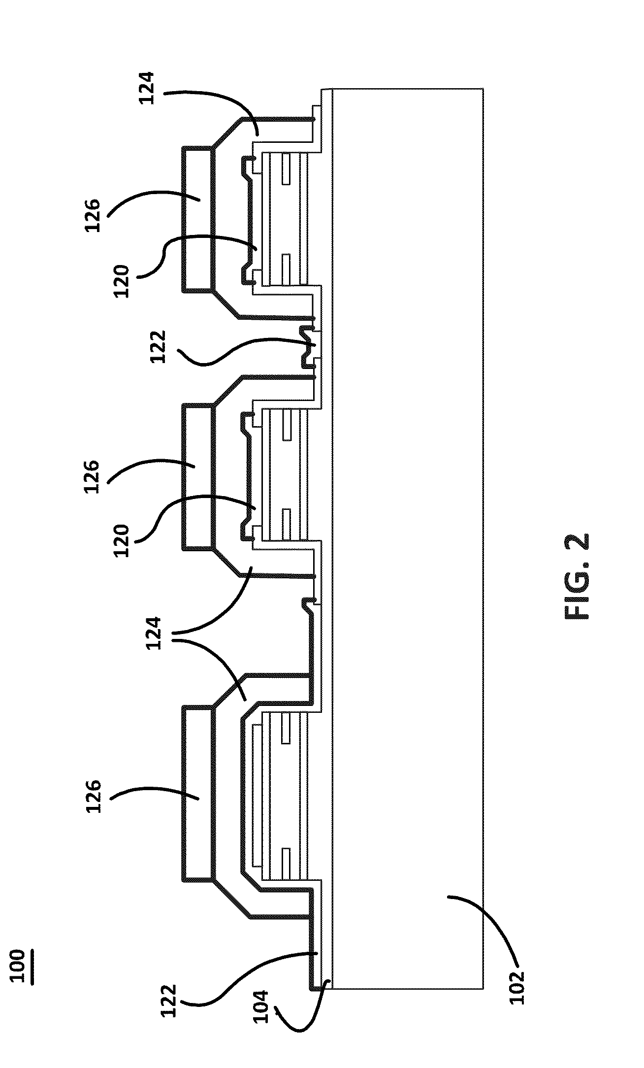
[0024]VCSEL array devices, such as those described in U.S. Pat. No. 5,812,571, are flip chip VCSEL array devices that employ a metal contact layer that is also used as a reflector for the top mirrors, and which is formed over each of the mesas. This single metal layer is customarily deposited with techniques such as electron beam (e-beam) evaporation or sputtering in order to create a highly uniform or reflective surface. Although these deposition techniques are normal for the stated application, they are not appropriate when seeking to achieve a thick metal layer encompassing the mesa, which is crucial for improved heat reduction in such devices. In order to use existing techniques to deposit a sufficiently thick layer, a large amount of metal must be used, such as Gold (Au), which significantly raises the cost of such devices. This type of design, and the design of other existing VCSEL array devices, also raises the overall impedance of the system and complicates heat management, ...


PUM


Abstract

A VCSEL array device formed of a monolithic array of VCSELs and short circuited mesas is disclosed. The VCSELs can be spaced symmetrically or asymmetrical, in a manner to improve power or speed, or in phase and in parallel. The VCSELs are connected to a first metal contact pad formed on a heat-spreading substrate. The short-circuited mesas are formed alongside the VCSELs and are bonded to and form a short circuit to a second metal contact pad on the grounding substrate. Each VCSEL is encompassed by a thick metal heat sink to increase the height of VCSEL mesas. The structure of the heat sink, the VCSELs and the shorting mesas reduce parasitic impedance thereby increasing output power and high frequency response. The VCSELs and shorting mesas can be packaged as a coplanar waveguide in a ground-signal-ground configuration that improves signal modulation characteristics.

Description

CROSS-REFERENCES TO RELATED APPLICATIONS[0001]This is a non-provisional application taking priority from provisional application Ser. No. 61 / 153,190, filed 17 Feb. 2009, which provisional application is incorporated herein by reference.BRIEF DESCRIPTION OF THE INVENTION[0002]An embodiment relates to semiconductor devices and, more particularly, to multibeam arrays of photonic devices for high power and high frequency applications, and methods of making and using the same.[0003]An embodiment is directed to a multibeam optoelectronic device, referred to as a VCSEL array device, which has high power and a high frequency response. The VCSEL array device is a monolithic array of VCSELs comprised of two or more VCSELs and an array of short-circuited mesa devices. The VCSELs of the VCSEL array can be spaced symmetrically or asymmetrical, spaced according to a mathematical function for improving a power or speed characteristic, or positioned for phase relationships next to each other in an ...

Claims


Application Information

Patent Timeline
IPC IPC(8): H01S3/04H01S5/183
CPCH01S5/0014H01S5/005H01S5/0224H01S5/02272H01S5/02276H01S5/02469H01S5/06226H01S5/18311H01S5/18347H01S5/423H01S2301/176H01S5/0234H01S5/0237H01S5/02345
Inventor JOSEPH, JOHN
Owner LUMENTUM OPERATIONS LLC
Why Eureka
Try Eureka