Multi-layer opto-electronic substrates with electrical and optical interconnections and methods for making

a technology of optoelectronic substrates and optical interconnections, applied in the field of optoelectronic substrates, can solve the problems of reducing the area requirements of optical interconnections in implementations using light modulators, and affecting the performance of optical interconnections. , to achieve the effect of reducing the area requirements, increasing the power of optical signals, and reducing nois

Inactive Publication Date: 2005-01-18
FUJITSU LTD
View PDF115 Cites 257 Cited by
  • Summary
  • Abstract
  • Description
  • Claims
  • Application Information

AI Technical Summary

Benefits of technology

One aspect of the present invention eliminates the need for the bulky drivers and amplifiers, which significantly reduces area requirements. In the place of a light-emitting source, the combination of an external light-source and an optical switch device (e.g., modulator) is used. The optical switch device is responsive to an output of an IC chip, and does not required a driver chip for operation. In contrast to light emitting source cases, the power of optical signals in implementations using light modulators can be greatly increased by increasing the size and power of the external light source. The external light source can be easily increased in this manner since it does not need to be modulated. For example, it can be implemented as a simple continuous wave (CW) or pulse trains source of optical power. In addition, losses in the optical connection are reduced. Therefore, and power at the photo-detectors is increased, which enables the amplifiers to be eliminated. The losses are reduced by integrally forming polymeric waveguides with the optical switches and the photo-detectors, which increases optical coupling efficiency. Additionally, the construction methods of the present invention enable short optical connections to he made. Optical power to the photo-detector device is increased by using the external optical power. In addition, optical waveguide integration methods of the present invention enable highly efficient optical connections to be made to VCSEL and laser-diode (LD) emitter devices, which enables these devices to be used as sources of optical power in addition to external sources.

Problems solved by technology

With the increase in clock rates and I / O counts of processing systems implemented on interconnection substrates, the problems of interconnection bottlenecks, noise, signal attenuation, heat generation, and maintaining synchronizable connection lengths in the electrical connections of such systems are appearing.
However, there is a large barrier which prevent optical interconnections from being used in high-speed digital / analog systems.
Thus far, bulky driver chips and amplifier chips have been required to provide the conversions between the optical signals in the optical interconnects and the electrical signals which are generated and used by the electronic chips.
The amplifier is needed because the light power becomes small at the photo-detector device due to considerable loss in conventional optical paths.
The driver and amplifier components require space on the circuit substrate, and therefore represent barriers to using large numbers of optical connections in a substrate, like a multichip module.
These excess components and their assembling increase manufacturing costs.
Furthermore, the conventional optical connections have longer delay due to EO and OE conversions, which would not provide significant speed benefits over pure electrical modules.

Method used


Image

  • Multi-layer opto-electronic substrates with electrical and optical interconnections and methods for making
  • Multi-layer opto-electronic substrates with electrical and optical interconnections and methods for making
  • Multi-layer opto-electronic substrates with electrical and optical interconnections and methods for making

Examples


first embodiment

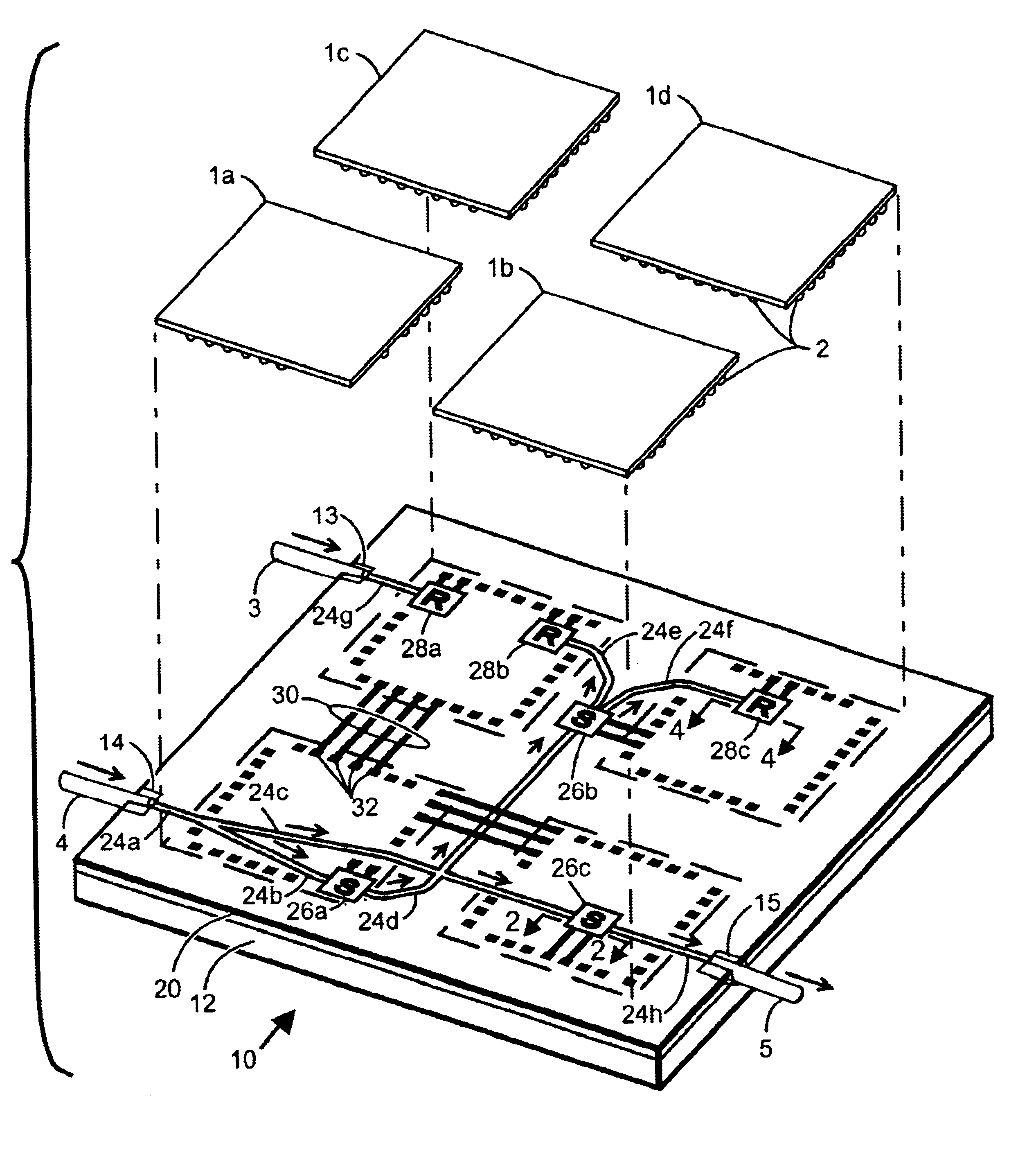
FIG. 1 shows an expanded perspective view of an opto-electronic (optical-electronic) interconnect substrate according to the present invention at reference number 10. The interconnect substrate 10 takes the form of an opto-electronic multichip module (OE-MCM) substrate that interconnects signal from one or a plurality of I.C. chips 1a-1d, including both inter-chip and intra-chip connections, by both optical links and electrical traces. Substrate 10 comprises a base substrate 12 and an active layer 20. The active layer comprises optical waveguides 24a-24h, opto-electronic switching devices 26a-26c, photo-detector devices 28a-28c, electrical traces 30, and electrical connection pads 32 for the I.C. chips 1. The I.C. chips are flip-chip assembled to active layer 20 and are electrically coupled to the connection pads 32 of layer 20 by a plurality of any type of conventional connectors 2. For the example, as shown in FIG. 1, connectors 2 may comprise solder bumps. The optical waveguides ...

second embodiment

FIG. 6 shows an expanded perspective view of an opto-electronic interconnect substrate according to the present invention at reference number 10′. The interconnect substrate 10′ is similar to substrate 10 shown in FIG. 1, and takes the form of an (opto-electronic multichip module OE-MCM) substrate that interconnects signal from one or a plurality of I.C. chips 1a-1d by both optical links and electrical traces. Common reference numbers have been used to designate common elements of substrates 10′ and 10. As one difference, substrate 10′ uses light emitting devices 36a and 36b in place of the opto-electronic switch devices 26a and 26b of substrate 10. The light emitting devices 36 do not need an outside source of light, such as provided by optical fiber 4 of substrate 10, and thus substrate 10′ does not require optical fiber 4. Device 36 may comprise a light-emitting diode (LED), a laser diode (LD), a vertical cavity surface emitting laser (VCSEL), quantum-well or quantum-dot devices ...


PUM


Abstract

Opto-electrical systems having electrical and optical interconnections formed in thin layers are disclosed. In one set of preferred embodiments, optical signals are conveyed between layers by respective vertical optical couplers disposed on the layers. In other preferred embodiments, optical signals are conveyed by stack optical waveguide coupling means. Yet other preferred embodiments have electrical via means formed in one or more layers to covey electrical signals between two or more layers.

Description

FIELD OF THE INVENTIONThe present invention relates to opto-electronic substrates that may be used to connection digital and / or analog electronic systems, and methods for making such systems. More specifically, the present invention relates to opto-electronic substrates that have both electrical and optical interconnections, and methods for making such substrates. The present invention may be applied to multichip modules (MCMs) and the like.BACKGROUND OF THE INVENTIONWith the increase in clock rates and I / O counts of processing systems implemented on interconnection substrates, the problems of interconnection bottlenecks, noise, signal attenuation, heat generation, and maintaining synchronizable connection lengths in the electrical connections of such systems are appearing. An optical interconnect has the advantage of low RC delay, low signal attenuation, predictable delay, low power, low noise and high tolerance to opens and shorts. However, there is a large barrier which prevent o...

Claims


Application Information

Patent Timeline
Patent Type & Authority Patents(United States)
IPC IPC(8): G02B6/13G02B6/132G02B6/12G02B6/42G02B6/43H01L23/538H01L23/48H01L23/52H01L25/16H01L21/68H01L21/67H01L31/12G02B6/122H01L21/60
CPCG02B6/12002G02B6/132G02B6/4214G02B6/43H01L23/48H01L23/5389H01L24/18H01L24/82H01L25/167H01L2924/10253H01L21/6835H01L2221/68345H01L2221/6835H01L2221/68359H01L2221/68368H01L2224/16225H01L2224/18H01L2924/01002H01L2924/01004H01L2924/0101H01L2924/01013H01L2924/01015H01L2924/01018H01L2924/01027H01L2924/01029H01L2924/0103H01L2924/01032H01L2924/01039H01L2924/01046H01L2924/01049H01L2924/01074H01L2924/01078H01L2924/01079H01L2924/01082H01L2924/10329H01L2924/10336H01L2924/12044H01L2924/14H01L2924/19041H01L2924/19043H01L2924/30105H01L2924/3011H01L2924/3025H01L2924/01005H01L2924/01006H01L2924/01023H01L2924/01024H01L2924/01033H01L2924/01047H01L2924/014H01L2924/12041H01L2924/00H01L2924/15788H01L2924/12043H01L2224/05573H01L2224/05568H01L2224/05147H01L2224/05184H01L2224/05644H01L2224/05647H01L2924/3512H01L2224/04105H01L2224/32225H01L2224/73267H01L2224/92244H01L21/568H01L2224/24137H01L24/19H01L24/05H01L2924/00014
Inventor YOSHIMURA, TETSUZOTAKAHASHI, YASHUHITOINAO, MASAAKILEE, MICHAEL G.CHOU, WILLIAMBEILIN, SOLOMON I.WANG, WEN-CHOU VINCENTROMAN, JAMES J.MASSINGILL, THOMAS J.
Owner FUJITSU LTD
Why Eureka
Try Eureka