Display panel driving circuit having charge sharing switch formed in pad

a technology of charge sharing switch and driving circuit, which is applied in the direction of electric digital data processing, instruments, computing, etc., can solve the problems of limit in the area of the chip, and achieve the effect of reducing the area required and reducing power consumption

Inactive Publication Date: 2011-07-14
SILICON WORKS CO LTD
View PDF3 Cites 17 Cited by
  • Summary
  • Abstract
  • Description
  • Claims
  • Application Information

AI Technical Summary

Benefits of technology

[0014]Accordingly, the present invention has been made in an effort to solve the problems occurring in the related art, and an object of the present invention is to provide a display panel driving circuit having charge sharing switches formed in pads, wherein charge sharing switches are formed in pads to decrease an area required for forming ESD (electrostatic discharge) protection devices and a heat value and reduce power consumption.

Problems solved by technology

However, since the charge sharing switches 131, 132 and 133 occupy a substantial portion of a chip area, limitations exist in decreasing the chip area.

Method used


Image

  • Display panel driving circuit having charge sharing switch formed in pad
  • Display panel driving circuit having charge sharing switch formed in pad
  • Display panel driving circuit having charge sharing switch formed in pad

Examples


Embodiment Construction

[0023]Reference will now be made in greater detail to a preferred embodiment of the invention, an example of which is illustrated in the accompanying drawings. Wherever possible, the same reference numerals will be used throughout the drawings and the description to refer to the same or like parts.

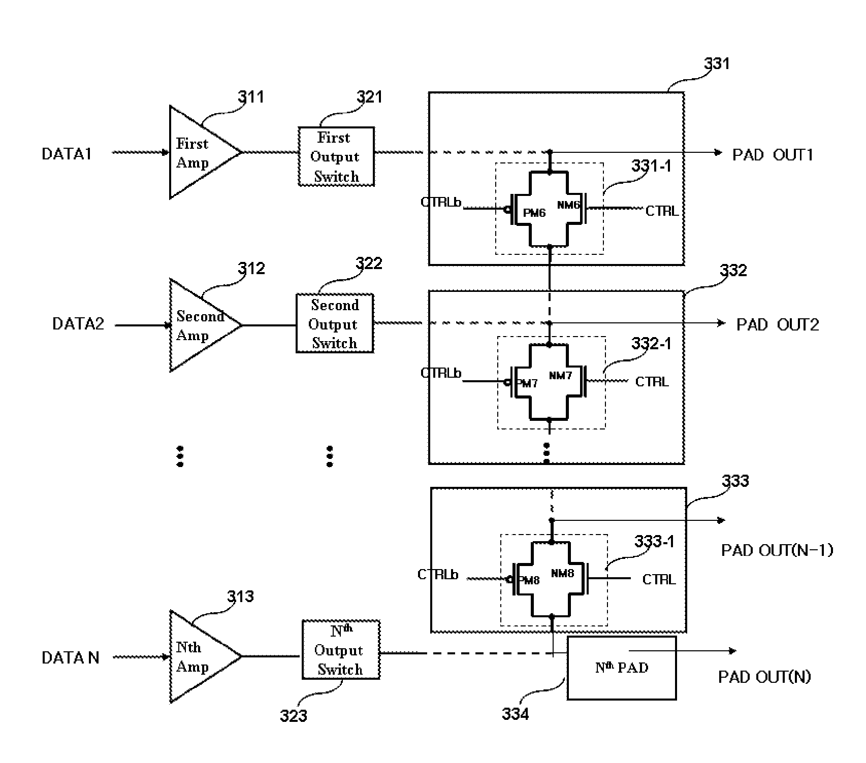
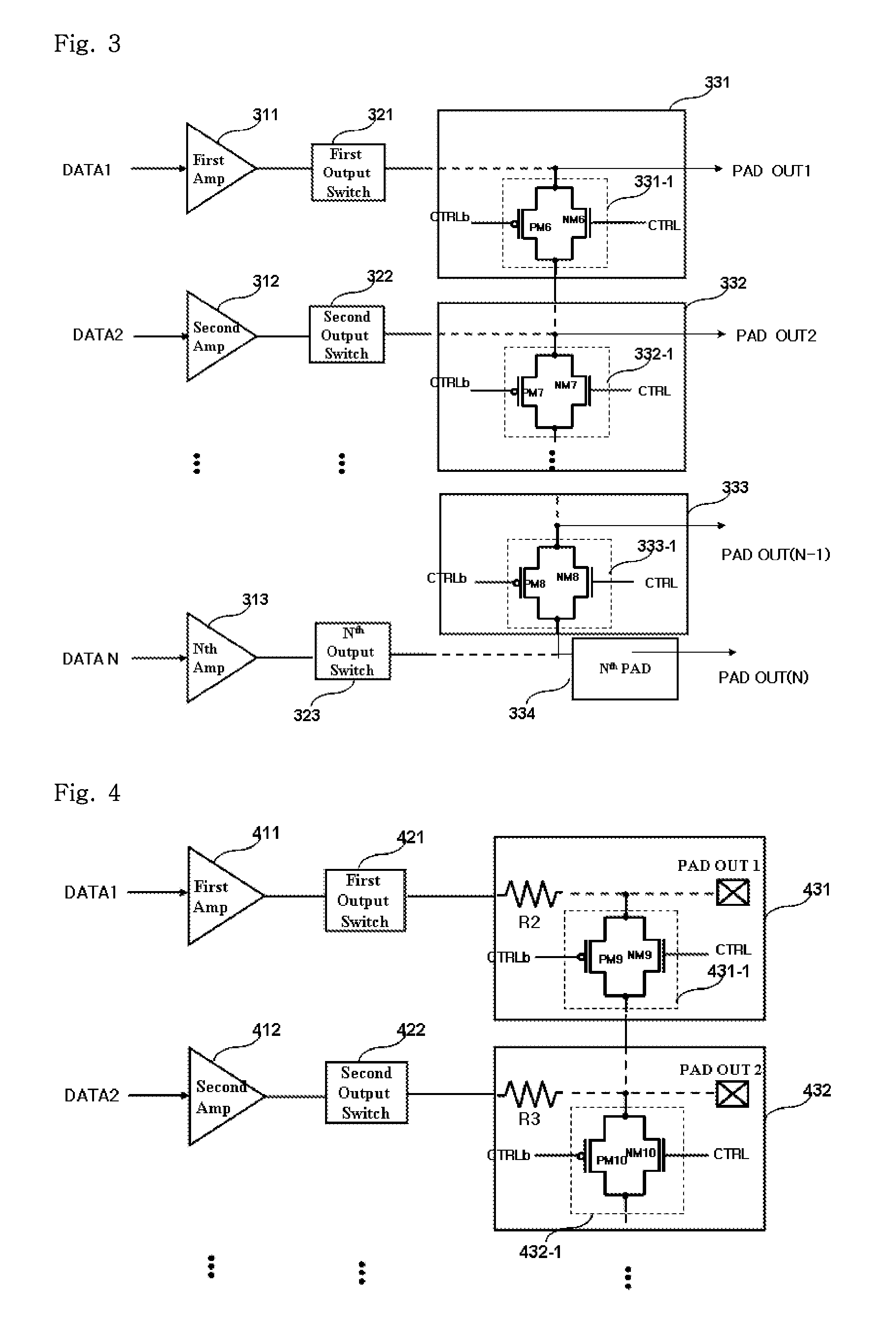
[0024]FIG. 3 is a diagram illustrating a display panel driving circuit having charge sharing switches formed in pads in accordance with an embodiment of the present invention.

[0025]Referring to FIG. 3, a display panel driving circuit having charge sharing switches formed in pads in accordance with an embodiment of the present invention includes N number of amplifiers 311, 312 and 313, N number of output switches 321, 322 and 323, N number of pads 331, 332, 333 and 334, and charge sharing switches 331-1, 332-1 and 333-1 which are formed in the pads 331, 332 and 333.

[0026]In the display panel driving circuit having charge sharing switches formed in pads, charge sharing switches are formed in...


PUM


Abstract

A display panel driving circuit includes N number of amplifiers configured to supply N number of output voltages to a display panel; N number of output switches configured to transmit output signals from the N number of amplifiers through N number of pads to the display panel; and a plurality of charge sharing switches configured to share charges among the N number of pads, wherein the charge sharing switches are formed in the pads.

Description

BACKGROUND OF THE INVENTION[0001]1. Field of the Invention[0002]The present invention relates to a display panel driving circuit, and more particularly, to a display panel driving circuit having charge sharing switches formed in pads, wherein charge sharing switches are formed in pads to serve as ESD (electrostatic discharge) protection devices and decrease an area and a heat value.[0003]2. Description of the Related Art[0004]In general, a semiconductor device is provided with pads for electrically connecting the semiconductor device with an outside. Signals associated with command input and data input / output operations are inputted to or outputted from the semiconductor device through the pads.[0005]Recently, as a design rule of a semiconductor device shrinks, a semiconductor manufacturing technology has been developed to accommodate a trend toward high integration. The size of a semiconductor device is scaled down due to the high integration, and the number of net dies manufacture...

Claims


Application Information

Patent Timeline
Patent Type & Authority Applications(United States)
IPC IPC(8): G09G5/00
CPCG09G3/20G09G2310/0254G09G2330/04G09G2330/023G09G2310/0275
Inventor JIN, BYUNG-YUNPARK, JONG-GEUNCHO, HYUN-HOCHOI, JOUNG-CHEULNA, JOON-HO
Owner SILICON WORKS CO LTD
Why Eureka
Try Eureka