Nitride semiconductor laser device

a laser device and semiconductor technology, applied in semiconductor lasers, lasers, active medium materials, etc., to achieve the effects of reducing ripples, good optical confinement, and enhancing etching precision

Inactive Publication Date: 2006-04-13
NICHIA CORP
View PDF99 Cites 258 Cited by
  • Summary
  • Abstract
  • Description
  • Claims
  • Application Information

AI Technical Summary

Benefits of technology

[0007] That is, according to the present invention, the waveguide having such stripe width and depth enables the basic mode emission having a stable lateral mode and there is no kink in the wide light output power range, resulting in a semiconductor laser device having a longer lifetime under continuous-wave operation.
[0029] Further, the fourth object of the present invention is to enhance the output power and reliability of the laser device according to the present invention.

Problems solved by technology

As mentioned above, the next problem the nitride semiconductor device which can realize continuous-wave oscillation is to raise the power of the device, in order to put the device to practical use and expand the application fields.
However, when the injection current into the laser device is increased and the optical power is increased, there is generally a kink due to the instability of the lateral mode, subsequently to the linear region after the initiation of oscillation, in the current—optical power characteristics.

Method used


Image

  • Nitride semiconductor laser device
  • Nitride semiconductor laser device
  • Nitride semiconductor laser device

Examples


embodiment 1

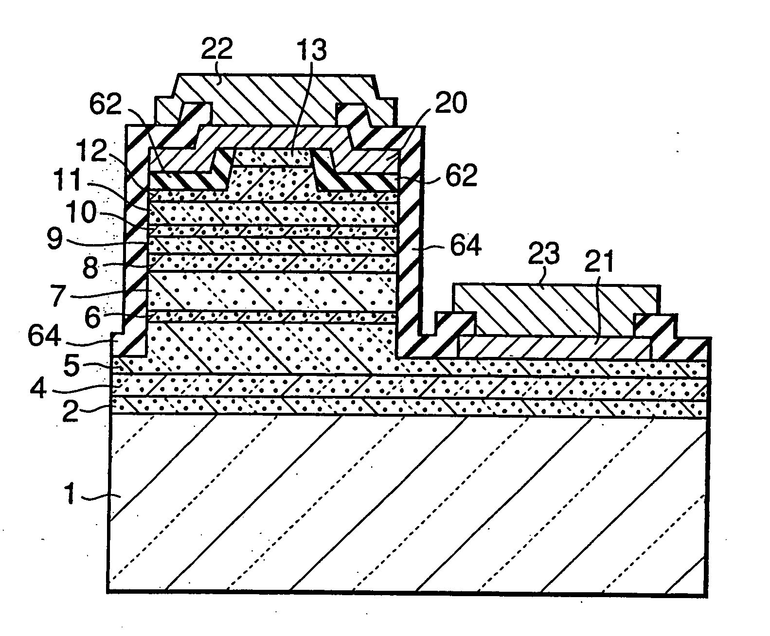
[0052] The etching operation employed to form the stripe-shaped waveguide region in the present invention is such an etching operation that forms a ridge waveguide having a cross section, for example, as shown in FIG. 1, that will be described in detail below following the p-side cladding layer and the p-side contact layer.

[0053] The nitride semiconductor laser device of the present invention comprises an active layer with at least the p-side first cladding layer and the p-side second cladding layer stacked thereon successively, while the layers are etched from the p-side contact layer side thereby to form the stripe-shaped waveguide region.

[0054] According to the present invention, there is required no particular layer between the active layer and the p-side cladding layer, although a guide layer and / or a cap layer (in case the cap layer is provided separately from-the cladding layer, the cap layer means the first cladding layer for carrier confinement and the cladding layer mean...

embodiment 2

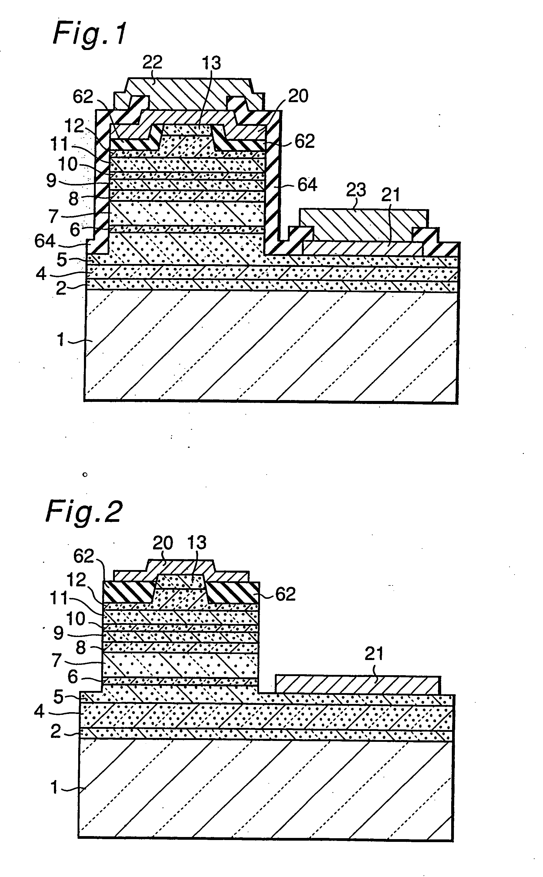
[0078] An embodiment of the present invention is shown in FIG. 17. Using this example, the present invention will be described in detail. The nitride semiconductor laser device of the present invention comprises an n-type nitride semiconductor layer, an active layer and a p-type nitride semiconductor layer stacked on a substrate, and has ridge structure of stripe shape formed by etching from the p-type nitride semiconductor side.

(Stripe-Shaped Waveguide Region)

[0079] The nitride semiconductor laser device of the present invention has a ridge waveguide formed on the p-side optical guide layer upward over the active layer. That is, an n-side optical guide layer made of n-type nitride semiconductor, the active layer and the p-side optical guide layer made of p-type nitride semiconductor are stacked on the substrate, wherein the p-side optical guide layer has a protruding portion of stripe shape and a stripe-shaped waveguide region. The laser device of the present invention is a refr...

embodiment 3

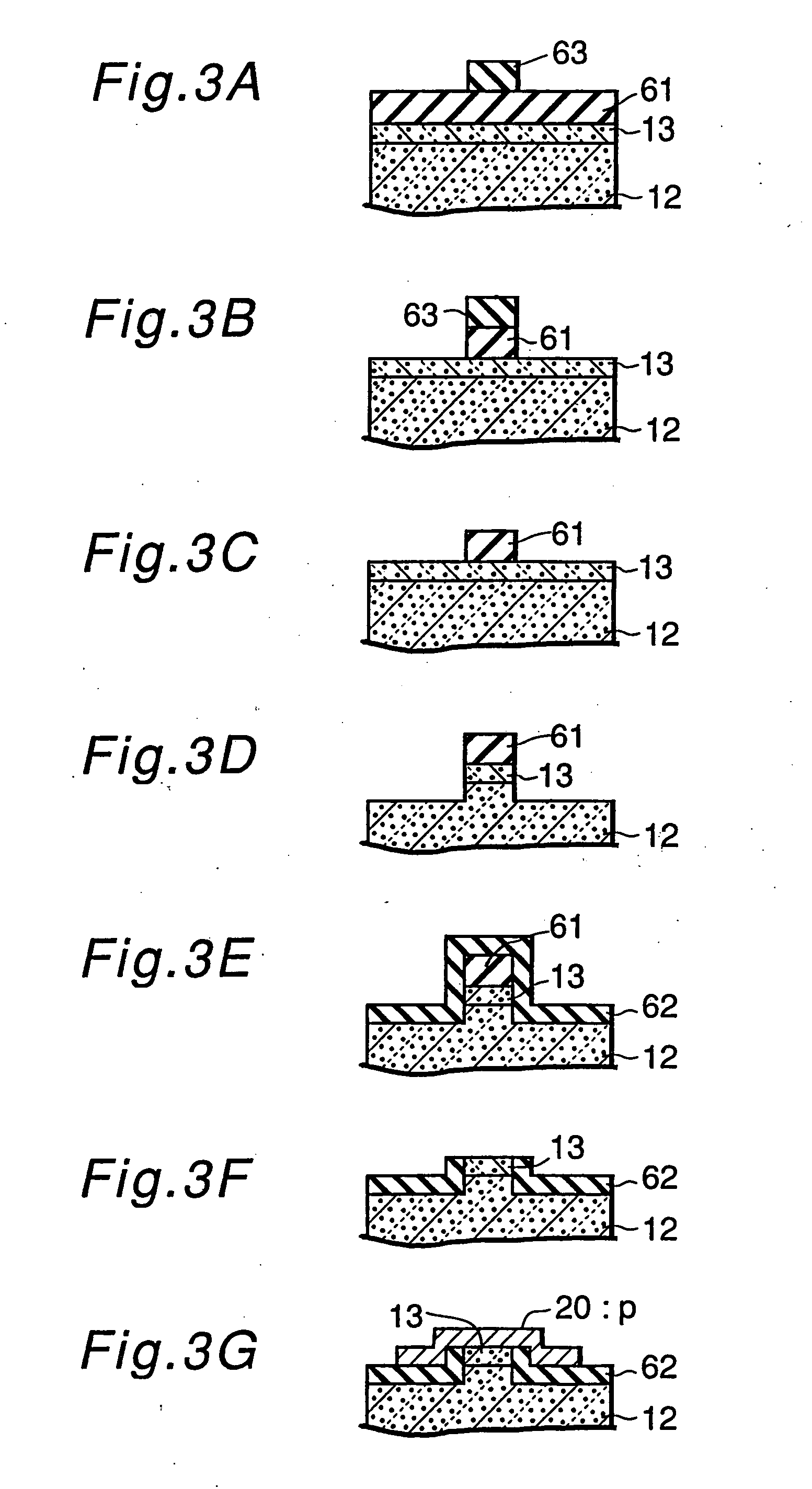
[0099] One embodiment of the present invention will now be described below by way of: a specific example. The nitride semiconductor laser device of the present invention has such a structure as the n-side optical guide layer made of n-type nitride semiconductor, the active layer and the p-side optical guide layer made of p-type nitride semiconductor are stacked on the substrate, similarly to that of the second layer made of n-type nitride semiconductor, the active layer and the p-side optical guide layer made of p-type nitride semiconductor are stacked on the substrate, wherein the p-side optical guide layer has a protruding portion of stripe shape and the stripe-shaped waveguide region is provided. The laser device of the present invention has the p-type nitride semiconductor layer formed on the protruding portion, and is specifically a refractive index guiding type laser device having the stripe-shaped waveguide region.

(Depth of Etching)

[0100] The laser device of the present in...


PUM


Abstract

A nitride semiconductor laser device has an improved stability of the lateral mode under high output power and a longer lifetime, so that the device can be applied to write and read light sources for recording media with high capacity. The nitride semiconductor laser device includes an active layer, a p-side cladding layer, and a p-side contact layer laminated in turn. The device further includes a waveguide region of a stripe structure formed by etching from the p-side contact layer. The stripe width provided by etching is within the stripe range of 1 to 3 μm and the etching depth is below the thickness of the p-side cladding layer of 0.1 μm and above the active layer. Particularly, when a p-side optical waveguide layer includes a projection part of the stripe structure and a p-type nitride semiconductor layer on the projection part and the projection part of the p-side optical waveguide layer has a thickness of not more than 1 μm, an aspect ratio is improved in far field image. Moreover, the thickness of the p-side optical waveguide layer is greater than that of an n-side optical waveguide layer.

Description

TECHNICAL FIELD OF THE INVENTION [0001] This invention relates to a nitride semiconductor laser device and particularly, to a laser device having an effective refractive index type narrow stripe ridge structure, which is used in an optical information processing field and can realize a continuous-wave operation at a high power without a kink. BACKGROUND OF THE INVENTION [0002] As the information-oriented society has developed in recent years, a φ device which can store a large amount of information has been required. Particularly, the layer light source having a short wavelength is longed for as a light source for a large amount media such as DVD and as a light source for communication. The applicators reported a nitride semiconductor layer device having a lifetime of ten thousand hours or more under room-temperature continuous-wave operation of in the single mode at the wavelength of 403.7 nm. [0003] As mentioned above, the next problem the nitride semiconductor device which can re...

Claims


Application Information

Patent Timeline
Patent Type & Authority Applications(United States)
IPC IPC(8): H01S5/00H01S5/20H01S5/22H01S5/223H01S5/32H01S5/323
CPCB82Y20/00H01S5/0655H01S5/2004H01S5/2031H01S5/22H01S5/2214H01S2304/00H01S5/223H01S5/2231H01S5/3213H01S5/32341H01S5/34333H01S5/2216H01S5/04257H01S5/04252H01S5/30
Inventor KOZAKI, TOKUYASANO, MASAHIKONAKAMURA, SHUJINAGAHAMA, SHINICHI
Owner NICHIA CORP
Why Eureka
Try Eureka