
Trench etching method and semiconductor device manufacturing method

A trench and photolithography technology, applied in semiconductor/solid-state device manufacturing, electrical components, circuits, etc., can solve the problem of inability to accurately control and dynamically adjust the key dimensions of the trench opening

Active Publication Date: 2017-07-11
SHANGHAI HUAHONG GRACE SEMICON MFG CORP
View PDF3 Cites 0 Cited by
  • Summary
  • Abstract
  • Description
  • Claims
  • Application Information

AI Technical Summary

Problems solved by technology

[0004] However, with the development of device design and manufacturing technology, and the improvement of electronic design requirements for device dimensional accuracy, it is often desired to be able to precisely control the critical dimensions of the trench opening, and the above-mentioned prior art trench etching method can only The critical dimension of the trench opening is roughly defined, but the critical dimension of the trench opening cannot be precisely controlled or dynamically adjusted

Method used


Image

  • Trench etching method and semiconductor device manufacturing method
  • Trench etching method and semiconductor device manufacturing method
  • Trench etching method and semiconductor device manufacturing method

Examples


Embodiment Construction

[0026] In order to make the content of the present invention clearer and easier to understand, the content of the present invention will be described in detail below in conjunction with specific embodiments and accompanying drawings.

[0027] Figure 1 to Figure 7 It schematically shows a structure diagram of a semiconductor device obtained by each step of the trench etching method according to an embodiment of the present invention.

[0028] Specifically, the trench etching method according to the embodiment of the present invention includes the following steps:

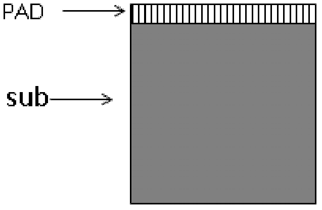
[0029] a pad oxide layer forming step, for forming a pad oxide layer PAD on the substrate sub, figure 1 The structure of the semiconductor device obtained after the pad oxide layer forming step is schematically shown. In a specific example, the thickness of the pad oxide layer PAD is, for example, 110A.

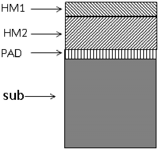
[0030] a hard mask forming step, for forming a hard mask (HM1, HM2) on the pad oxide layer PAD, figure 2 Th...


PUM


Abstract

The invention provides a groove etching method and a semiconductor device manufacturing method. The trench etching method according to the present invention includes: a pad oxide layer forming step for forming a pad oxide layer on a substrate; a hard mask forming step for forming a hard mask on the pad oxide layer The photoresist layer forming step is used to form a photoresist layer on the hard mask; the photolithography step is used to photoetch the photoresist layer to obtain the pattern of the photoresist layer; hard mask etching Etching step, for utilizing the pattern of the photoresist layer obtained in the photolithography step to etch the hard mask to form a hard mask pattern; photoresist layer removal step, using oxygen to remove the photoresist layer and a trench etching step, for utilizing the hard mask pattern etched by the hard mask etching step to etch a trench with oxygen; wherein, by controlling the oxygen in the trench etching step The flow rate is used to control the critical dimension of the trenches etched in the trench etching step.

Description

technical field [0001] The invention relates to the field of semiconductor device manufacturing, more specifically, the invention relates to a trench etching method and a semiconductor device manufacturing method using the trench etching method. Background technique [0002] In the manufacturing process of various semiconductor devices, trench etching, such as shallow trench etching, is generally required. [0003] Generally, in the existing trench etching method, the photoresist is first photoetched, then the photoresist pattern after photoetching is used to etch the hard mask, and finally the etched hard mask is used to etch the hard mask. film pattern to etch trenches. Thus, lithography of the photoresist will then define a lithography CD, and after the hardmask etch a hardmask etch CD will be defined, the two CDs (i.e., the lithography CD and Hardmask Etch CD) essentially defines the final trench CD of the trench. [0004] However, with the development of device desig...

Claims


Application Information

Patent Timeline
Patent Type & Authority Patents(China)
IPC IPC(8): H01L21/027
Inventor 熊磊奚斐
Owner SHANGHAI HUAHONG GRACE SEMICON MFG CORP
Learn More