Manufacturing method of trench and manufacturing method of memory device

A manufacturing method and storage device technology, applied in the field of memory manufacturing and groove manufacturing, can solve problems such as the difficulty of critical dimensions of U-shaped grooves, increase effective current and read window, reduce channel length, Effects that improve resolution and fidelity

Pending Publication Date: 2022-02-01
WUHAN XINXIN SEMICON MFG CO LTD
View PDF0 Cites 1 Cited by
  • Summary
  • Abstract
  • Description
  • Claims
  • Application Information

AI Technical Summary

Problems solved by technology

It is difficult to further reduce the critical dimension (CD) of the U-shaped groove in the existing manufacturing process

Method used


Image

  • Manufacturing method of trench and manufacturing method of memory device
  • Manufacturing method of trench and manufacturing method of memory device
  • Manufacturing method of trench and manufacturing method of memory device

Examples


Embodiment Construction

[0049] For reference and clarity, descriptions, abbreviations or abbreviations of technical terms used hereinafter are summarized as follows:

[0050] BARC: Bottom Anti Reflection Coating;

[0051] DARC: Dielectric Anti Reflective Coating, dielectric anti-reflection coating;

[0052] ODL: Organic Dielectric Layer, organic underlying structure layer;

[0053] SHB: Si-O-based Hard Mask, silicon oxide hard mask interlayer structure layer.

[0054] As described in the background art, it is difficult to further reduce the critical dimension (CD) of the U-shaped trench in the existing semi-floating gate transistor fabrication process.

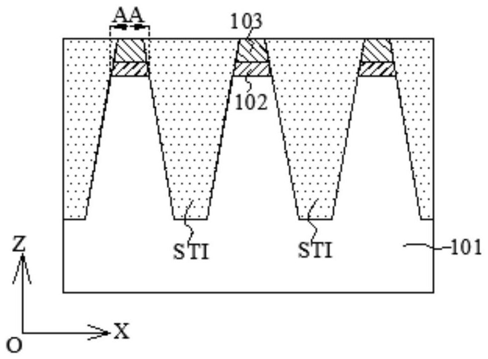
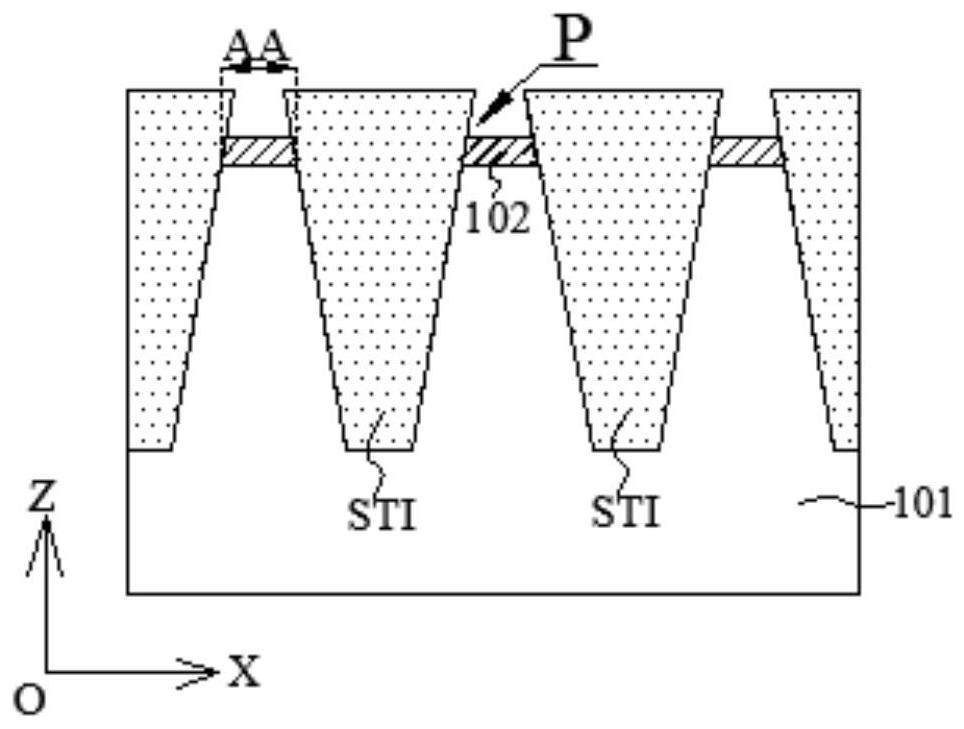
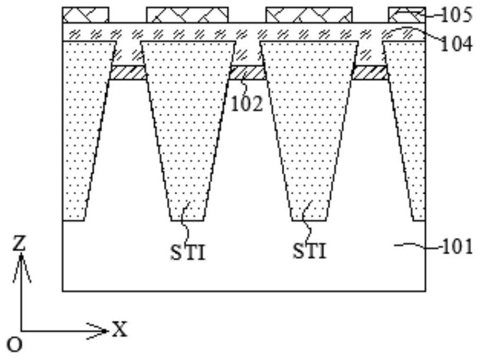
[0055] Specifically, an existing manufacturing process for a semi-floating gate transistor includes the following steps: Figure 1 to Figure 4 steps in .

[0056] like figure 1 As shown, a silicon oxide layer 102 and a silicon nitride layer 103 are sequentially formed on the substrate 101, and shallow trench isolation STIs are formed at interval...


PUM


Abstract

The invention provides a manufacturing method of a trench and a manufacturing method of a memory device. A mask layer comprises an amorphous carbon layer and a DARC layer which are stacked, and the amorphous carbon layer covers a shallow trench isolation layer and a nitride layer; before the mask layer is formed, the nitride layer is not removed, pits are prevented from being formed, the advantage of the high vertical and horizontal etching selection ratio of the amorphous carbon layer is utilized, and the defect that the filling capacity of the amorphous carbon layer is poor is overcome. According to the method, the photoresist layer and the mask layer are etched layer by layer to pattern the photoresist layer and the mask layer, the corresponding opening of the groove is etched by adopting a multi-layer film layer structure formed by overlapping the mask layer and the photoresist layer, and the pattern and size of the opening are sequentially transmitted, so that the resolution and fidelity of the opening pattern are improved, and the accurate control of the key size of the opening pattern is realized. Therefore, the key size of the trench can be accurately controlled, and the key size of the trench can be further reduced. The key size of the trench is reduced, and the channel length of the memory device is correspondingly reduced, so that the effective current and the read window of the memory device can be increased.

Description

technical field [0001] The present invention relates to the technical field of semiconductors, and in particular, to a method for fabricating a trench and a method for fabricating a memory. Background technique [0002] Semiconductor memories are used in various electronic fields. Among them, non-volatile memory can save data for a long time in the case of power failure. Floating gate transistors are a mainstream non-volatile memory. In general, floating gate transistors have a stacked gate structure comprising a floating gate (floating gate) and a control gate (control gate) at least partially covering the floating gate, wherein the floating gate is surrounded by an insulating dielectric , by applying a high voltage to control the carriers to pass through the gate insulating layer in the manner of tunneling or hot carrier injection, thereby changing the amount of stored charge in the floating gate, the threshold voltage of the transistor can be adjusted, that is, correspo...

Claims


Application Information

Patent Timeline
Patent Type & Authority Applications(China)
IPC IPC(8): H01L21/311H01L21/308H01L21/336H01L27/11521
CPCH01L21/31144H01L21/31105H01L21/3086H01L29/66825H10B41/30
Inventor 龚风丛
Owner WUHAN XINXIN SEMICON MFG CO LTD
Why Eureka
Try Eureka