
Manufacturing method of metal nanowire or sheet and nanowire or sheet

A metal nanowire and a manufacturing method technology, applied in the manufacture of metal nanowires or sheets, in the field of nanowires or sheets, can solve problems such as difficult etching, inability to flexibly control the width and thickness of nanowires, uncontrollable cross-sectional shape of nanowires, etc.

Active Publication Date: 2019-12-27
INST OF MICROELECTRONICS CHINESE ACAD OF SCI
View PDF8 Cites 2 Cited by
  • Summary
  • Abstract
  • Description
  • Claims
  • Application Information

AI Technical Summary

Problems solved by technology

With the research of advanced interconnection technology of integrated circuits, the research of Ru, Co, Mo and other metal nanowire materials has become a hot spot, but these materials are extremely difficult to etch no matter whether they are dry or wet.
At present, for Ru, Co and other metals, the methods of lift off, Damascene and sidewall transfer direct etching are mainly used. The resolution of the lift-off process is limited, and the Damascene process is complicated. The sidewall transfer is used to directly etch metal nanowires. The cross-sectional shape of the nanowire is uncontrollable, the width and thickness of the nanowire cannot be flexibly controlled, and there is plasma damage to the nanowire

Method used


Image

  • Manufacturing method of metal nanowire or sheet and nanowire or sheet
  • Manufacturing method of metal nanowire or sheet and nanowire or sheet
  • Manufacturing method of metal nanowire or sheet and nanowire or sheet

Examples


Embodiment 1

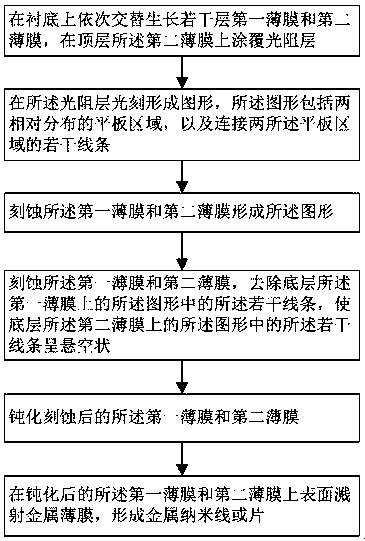
[0051] see Figure 1-Figure 4 , Figure 5A-Figure 9A , Figure 5B-Figure 9B and Figure 10 , the method includes:

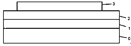
[0052] S101 : growing a first film 1 and a second film 2 sequentially on a substrate 0 , and coating a photoresist layer 3 on the second film 2 .

[0053] In the field of semiconductors, the substrate 0 may be understood as a base for forming transistors or other semiconductor devices thereon. On the one hand, the substrate 0 acts as a mechanical support, and a thin film is formed on the substrate 0 by physical or chemical means, and then semiconductor devices are formed by processes such as photolithography and atom implantation. On the other hand, the substrate 0 has the effect of improving the film properties. The film is formed on the substrate 0. The material properties of the substrate 0 and the surface shape of the substrate 0 have a great influence on the film properties. Since the film thickness is usually in the nanometer Between micron and micron,...

Embodiment 2

[0068] see figure 1 , Figure 11-Figure 18 , Figure 19A-Figure 22A , Figure 19B-Figure 22B and Figure 23 , the method includes:

[0069] S201: growing two layers of the first thin film 1 and the second thin film 2 alternately in sequence on the substrate 0, and coating the photoresist layer 3 on the second layer of the second thin film 2.

[0070] It should be noted that, in this embodiment, the first layer of the first thin film 1, the first layer of the second thin film 2, the second layer of the first thin film 1, and the second layer of the second thin film 2 are sequentially grown upward on the substrate 0 (see Figure 11 ), can also alternately grow three layers, four layers, etc. In this embodiment, chemical vapor deposition (CVD) is used for film growth. The first film 1 is SiO2 with a thickness of 50 nanometers, and the second film 2 is an amorphous Si film with a thickness of 100 nanometers.

[0071] After growing the first layer of the first thin film 1, th...


PUM

PropertyMeasurementUnit
thicknessaaaaaaaaaa
thicknessaaaaaaaaaa
diameteraaaaaaaaaa

Abstract

The invention provides a manufacturing method of a metal nanowire or sheet. The method comprises the following steps that: a plurality of layers of first films and second films are sequentially and alternately grown on a substrate, and the second film on the top layer of the substrate is coated with a photoresist layer; a pattern of which the two ends are flat areas is formed on the photoresist layer by means of photoetching, a plurality of lines being connected in the middle of the pattern; the first films and the second films are etched, so that the above pattern can be formed; the pluralityof lines on the first film at the bottom layer of the substrate is removed, so that a plurality of lines on the second film at the bottom layer to be suspended; and the etched first films and secondthin films are passivated, metal films are sputtered on the upper surfaces of the passivated first films and second films, so that naturally isolated metal nanowires or sheets can be formed. Accordingto the method, photoetching and film growth are performed; special etching is used in combination; the metal films can be sputtered on the upper surfaces of the passivated first film and second films; due to the fact that the coverage rate of a step formed through etching is limited, the natural physical isolation of the nanowires or sheets can be achieved, and extra process steps are not needed.The invention also provides a nanowire or a sheet.

Description

technical field [0001] The invention relates to the field of manufacturing semiconductor devices, in particular to a method for manufacturing metal nanowires or sheets and the nanowires or sheets. Background technique [0002] With the development of information technology, the requirements for the computing speed and integration level of semiconductor devices are gradually increased, and the critical dimensions (Critical Dimension, CD) of semiconductor devices are gradually reduced. Based on the user's demand for computing speed and integration, nanowires emerged as the times require. [0003] A nanowire refers to a one-dimensional structure that is confined to less than 100 nanometers in the lateral direction (with no restriction in the longitudinal direction). Suspended nanowires mean that the ends of the nanowires are fixed under vacuum conditions. A typical nanowire has an aspect ratio above 1000, so it is often regarded as a one-dimensional structure. With the resea...

Claims


Application Information

Patent Timeline
Patent Type & Authority Applications(China)
IPC IPC(8): H01L21/02B82Y40/00
CPCB82Y40/00H01L21/02697
Inventor 李俊杰刘耀东周娜王桂磊高建峰李永亮罗军赵超王文武
Owner INST OF MICROELECTRONICS CHINESE ACAD OF SCI
Learn More