Manufacturing method of groove and manufacturing method of memory device

A manufacturing method and storage device technology, which are applied in the field of storage device fabrication and trench fabrication, can solve problems such as difficulties, and achieve the effects of improving function, improving resolution and fidelity, and reducing etching rate.

Pending Publication Date: 2022-02-01
WUHAN XINXIN SEMICON MFG CO LTD
View PDF0 Cites 1 Cited by
  • Summary
  • Abstract
  • Description
  • Claims
  • Application Information

AI Technical Summary

Problems solved by technology

It is difficult to further reduce the critical dimension (CD) of the U-shaped trench in the existing semi-floating gate transistor manufacturing process

Method used


Image

  • Manufacturing method of groove and manufacturing method of memory device
  • Manufacturing method of groove and manufacturing method of memory device
  • Manufacturing method of groove and manufacturing method of memory device

Examples


Embodiment Construction

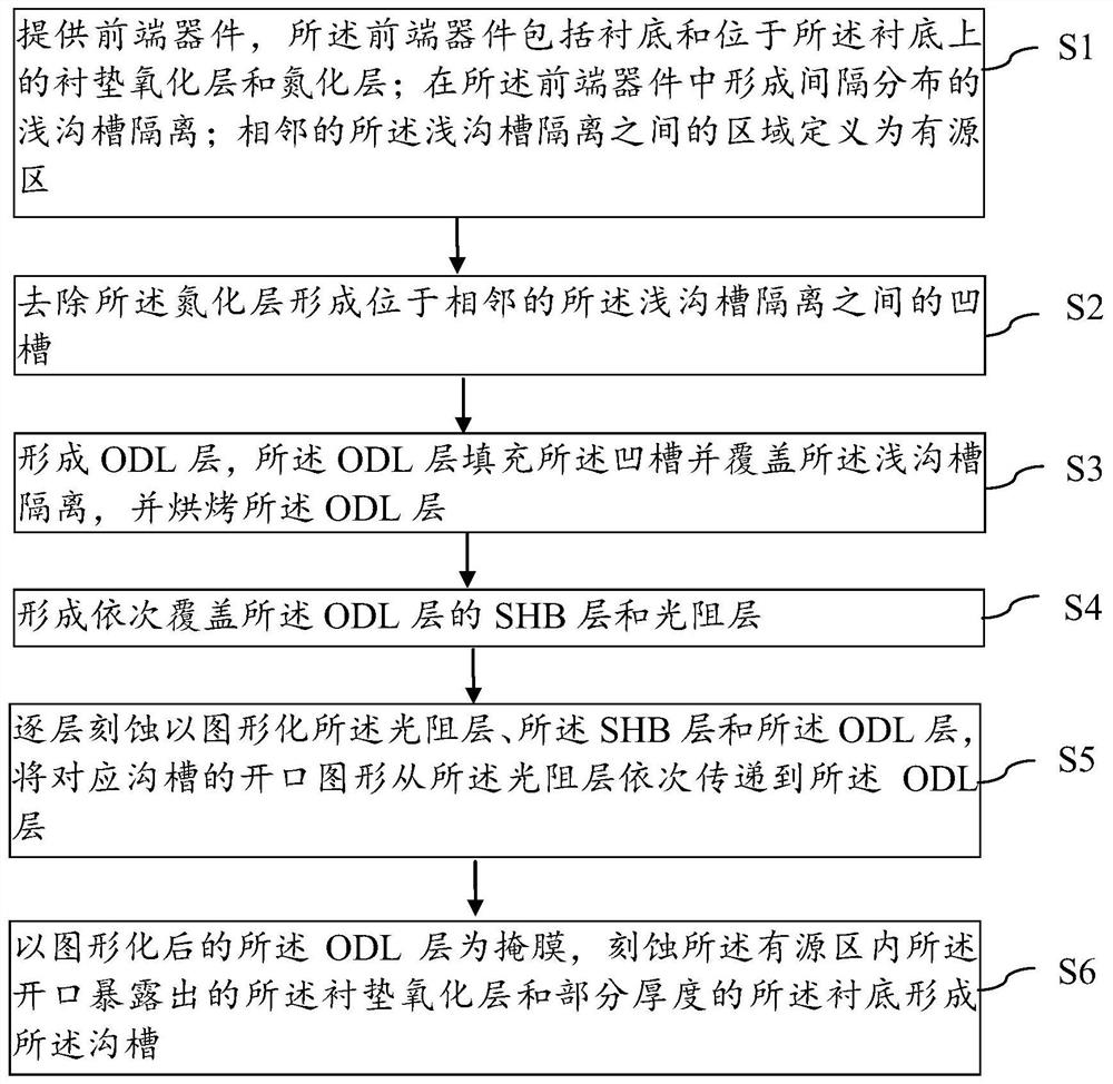
[0052] For reference and clarity, descriptions, abbreviations or abbreviations of technical terms used in the following text are summarized as follows:

[0053] BARC: Bottom Anti Reflection Coating, bottom anti-reflection coating;

[0054] ODL: Organic Dielectric Layer, organic dielectric layer;

[0055] SHB: Si-O-based Hard Mask, silicon oxide hard mask interlayer structure layer.

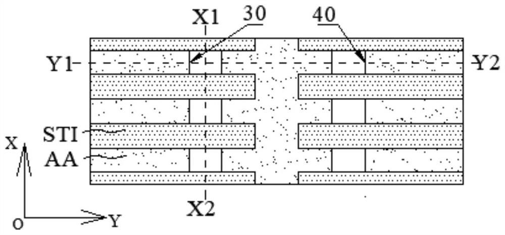
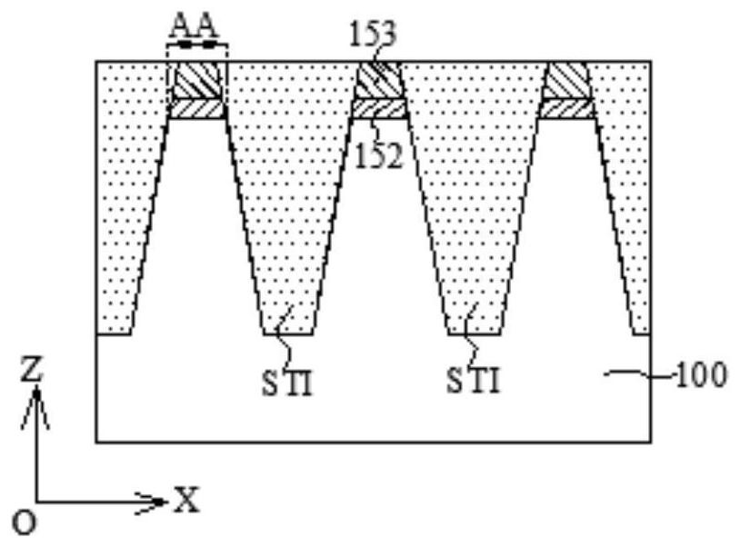
[0056] As mentioned in the background art, it is difficult to further reduce the critical dimension (CD) of the U-shaped trench in the existing semi-floating gate transistor manufacturing process. The main reason for restricting the shrinkage of the groove (U-shaped groove) is: the ODL layer, the mask layer for making the groove, is adopted due to its excellent step coverage performance, but its loose characteristics make it easy to be etched laterally. As a result, the CD of the trench is enlarged.

[0057] Specifically, use the ODL layer as a mask to etch the substrate to form a groove, and i...


PUM


Abstract

The invention provides a manufacturing method of a groove and a manufacturing method of a memory device. The manufacturing method comprises the following steps: providing a front-end device; forming an ODL layer; baking the ODL layer to enable the ODL layer to be more compact, and weakening the lateral etching rate; the opening of the corresponding groove formed in the ODL layer does not expand outwards and being not etched laterally, so that the key size of the opening corresponding to the groove is effectively controlled. A photoresist layer, an SHB layer and an ODL layer are etched layer by layer to pattern the photoresist layer, the SHB layer and the ODL layer, a multi-layer film layer structure is adopted to etch corresponding openings of a groove, the patterns and sizes of the openings are transmitted in sequence, the resolution and fidelity of the patterns of the openings are improved, accurate control over the key sizes of the patterns of the openings is achieved, and therefore the key sizes of the groove can be accurately controlled, and the key size of the groove can be further reduced. The key size of the groove is reduced, the channel length of the memory device is correspondingly reduced, a semi-floating gate buried channel with small size and effective vertical morphology is formed, the electrical performance of the semi-floating gate device is improved, and the yield of a memory device wafer is improved.

Description

technical field [0001] The invention relates to the technical field of semiconductors, in particular to a method for manufacturing a groove and a method for manufacturing a storage device. Background technique [0002] Semiconductor memories are used in various electronic fields. Among them, non-volatile memory can save data for a long time in the case of power failure. Semi-floating gate transistors are a mainstream non-volatile memory. The semi-floating gate transistor uses the quantum tunneling effect of the Tunneling Field-Effect Transistor (TFET) and the pn junction diode to replace the traditional silicon oxide erasing window to realize the charge and discharge of the floating gate, which can greatly reduce the transistor The working voltage is higher, and the working speed of the transistor is improved to realize faster data writing and erasing under low voltage, which is convenient to meet the needs of low power consumption of the chip. [0003] The semi-floating ...

Claims


Application Information

Patent Timeline
Patent Type & Authority Applications(China)
IPC IPC(8): H01L21/311H01L21/308H01L21/336H01L27/11521
CPCH01L21/31144H01L21/31105H01L21/3086H01L29/66825H10B41/30
Inventor 谢岩邹浩
Owner WUHAN XINXIN SEMICON MFG CO LTD
Why Eureka
Try Eureka