
Photoelectric conversion device

A technology for photoelectric conversion devices and photoelectric conversion layers, applied in photovoltaic power generation, circuits, electrical components, etc., can solve problems such as inability to obtain intermediate contact layers and small incident light

Inactive Publication Date: 2012-03-14
MITSUBISHI HEAVY IND LTD
View PDF4 Cites 0 Cited by
  • Summary
  • Abstract
  • Description
  • Claims
  • Application Information

AI Technical Summary

Problems solved by technology

However, in the single-layer intermediate contact layer, there is a problem that the amount of light incident on the crystalline silicon layer is extremely small
Even if the refractive index (intermediate contact layer material) and film thickness are adjusted, a single-layer intermediate contact layer with optimal selective reflection characteristics cannot be obtained

Method used


Image

  • Photoelectric conversion device
  • Photoelectric conversion device
  • Photoelectric conversion device

Examples


Embodiment 1

[0071] for Figure 6 In the stacked solar cell unit shown in the structural model, the optical analysis calculation based on the FDTD (Finite Difference Time Domain: finite difference in time domain) method is performed when light is incident from the glass substrate 1 side, and the light distribution of each layer is obtained. absorption spectrum. The value obtained by integrating the value obtained by multiplying the absorption spectrum by the sunlight spectrum (AM1.5) was defined as the current. The size of one pixel of the structural model is 10 nm. Assuming that the structural model is a pseudo-two-dimensional model, optical analytical calculations are performed for the two polarization directions of light (p-polarized light and s-polarized light), and the average of the two results is used as the solution. p-polarized light refers to the electric field vector relative to Figure 6 For polarized light parallel to the paper, s-polarized light refers to the electric fiel...

Embodiment 2

[0101] The configuration and film thickness of each layer in Example 2 are the same as those in Example 1.

[0102] In Example 2, the Figure 6 The haze value of the transparent electrode layer (substrate provided with the transparent electrode layer) of the structural model is set to 30%, the pitch of the concave-convex structure of the transparent electrode layer 2 is set to 1 μm, and the inclination angle is set to 30°. For the surface shapes of the i-layer 32 of the first unit layer and the i-layer 42 of the second unit layer, structural models obtained from the results of AFM shape analysis were used.

[0103] Regarding Example 2, the same short-circuit current distribution diagram as that of Example 1 was obtained by optical analysis calculation. In Example 2, the film thickness region where the short-circuit current increases tends to be slightly shifted toward the thinner side of the titanium oxide film than the film thickness region where the short-circuit current in...


PUM


Abstract

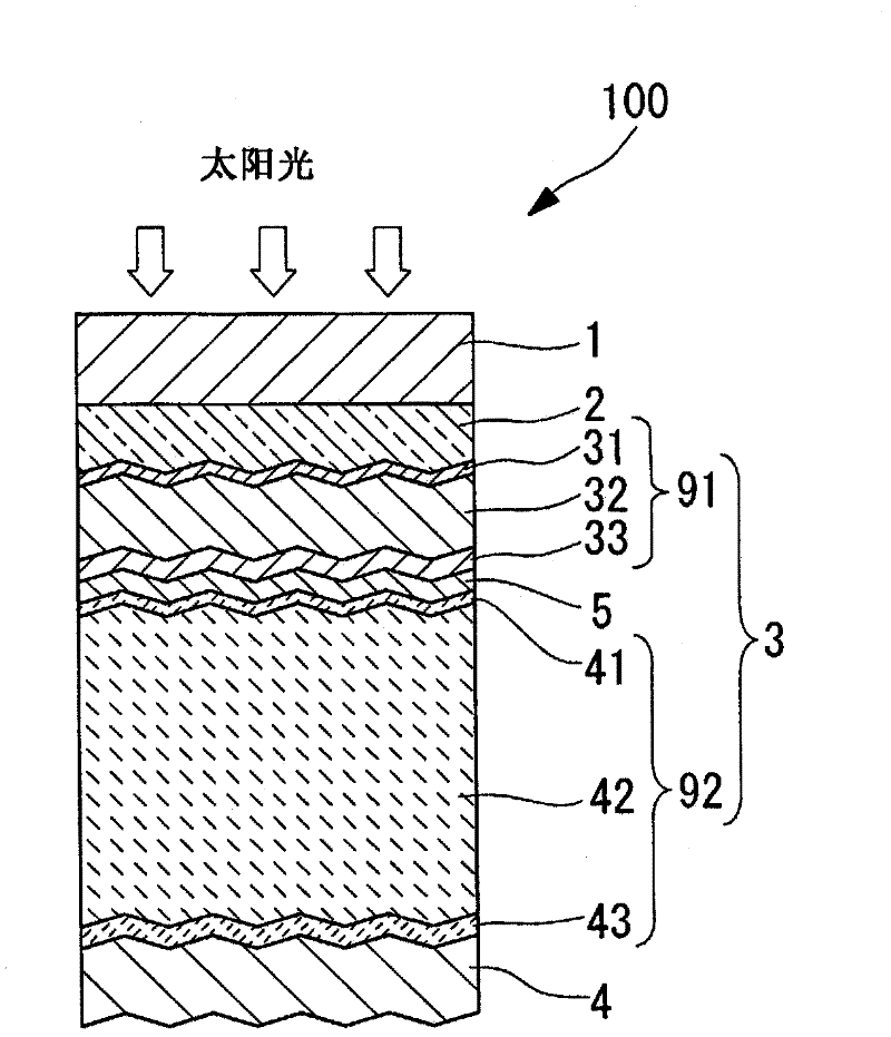
Provided is a photoelectric conversion device provided with an intermediate contact layer, the reflection characteristics of which are optimized. A photoelectric conversion device (100) is provided with a transparent electrode layer (2) which is provided on a substrate (1) and which is provided with an uneven structure on a surface opposite to the substrate (1), a photoelectric conversion layer (3) comprised of two power generation layers (91, 92), an underside electrode layer (4), and an intermediate contact layer (5) provided between the two power generation layers (91, 92). The intermediate contact layer (5) is comprised of a titanium oxide film mainly composed of titanium oxide, and an underside transparent conductive film mainly composed of transparent conductive oxide, in this order from the substrate (1) side. The thickness of the titanium oxide film is in a range of 65-110 nm inclusive when the thickness of the underside transparent conductive film is 5 nm, and likewise, 65-95 nm inclusive when 10 nm, 65-90 nm inclusive when 15 nm, 60-85 nm inclusive when 20 nm, 55-70 nm inclusive when 25 nm, and 55-65 nm inclusive when 30 nm.

Description

technical field [0001] The present invention relates to a photoelectric conversion device, in particular to a thin-film solar cell in which a power generation layer is produced by film formation. Background technique [0002] As a photoelectric conversion device that converts the energy of sunlight into electrical energy, there are known photoelectric conversion devices equipped with p-type silicon-based semiconductors (p layer), i-type silicon-based semiconductors (i-layer) and n-type silicon-based semiconductors produced by plasma CVD or the like. A thin-film silicon-based solar cell with a photoelectric conversion layer formed of a semiconductor (n-layer) thin film. Advantages of thin-film silicon-based solar cells include easy enlargement of the area, thin film thickness of about 1 / 100 of that of crystalline solar cells, and fewer materials. Therefore, thin-film silicon-based solar cells can be produced at a lower cost than crystalline solar cells. [0003] In this tec...

Claims


Application Information

Patent Timeline
Patent Type & Authority Applications(China)
IPC IPC(8): H01L31/04
CPCH01L31/022466H01L31/076Y02E10/548
Inventor 坂井智嗣小林靖之
Owner MITSUBISHI HEAVY IND LTD
Learn More