Processing method of optical device wafer

A processing method and technology of optical devices, applied in the fields of semiconductor devices, metal processing equipment, semiconductor/solid-state device manufacturing, etc., can solve the problems of electrode short circuit, quality degradation, squeezing, etc., to eliminate squeezing, ductility suppression, elimination The effect of electrodes short-circuiting each other

Active Publication Date: 2016-07-13
DISCO CORP
View PDF5 Cites 0 Cited by
  • Summary
  • Abstract
  • Description
  • Claims
  • Application Information

AI Technical Summary

Problems solved by technology

[0008] However, when the surface of the translucent molding resin is polished to expose the electrodes and the optical device wafer is finished to a desired thickness as described in Patent Document 1, there is a problem that the translucent molding resin has Surface cracking (mushire) and quality deterioration
[0009] In addition, if the translucent molding resin is covered in such a way that electrodes such as gold or platinum protruding from the n-type semiconductor layer and the p-type semiconductor layer are embedded, and then the surface of the translucent molding resin is polished so that the electrodes are separated from the If the translucent molding resin is exposed, there is a problem that the electrodes may be short-circuited due to the ductility of the metal.

Method used


Image

  • Processing method of optical device wafer
  • Processing method of optical device wafer
  • Processing method of optical device wafer

Examples


Embodiment Construction

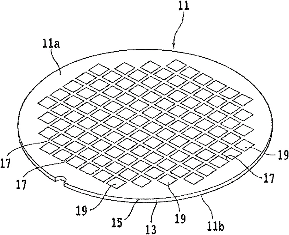
[0033] Hereinafter, embodiments of the present invention will be described in detail with reference to the drawings. refer to figure 1 , shows a front side perspective view of an optical device wafer. The optical device wafer 11 is formed by laminating an epitaxial layer (light emitting layer) 15 such as gallium nitride (GaN) on a sapphire substrate 13 . The optical device wafer 11 has: a surface 11 a formed by laminating light emitting layers 15 ; and a back surface 11 b exposed from the sapphire substrate 13 .

[0034] In the light-emitting layer 15 , a plurality of optical devices 19 such as LEDs are divided and formed by dividing lines (segments) 17 formed in a grid pattern. The optical device wafer 11 to be processed in the present invention is formed by covering the surface 11 a with a translucent molding resin (not shown).

[0035] That is, if Figure 8 As shown in the partially enlarged cross-sectional view of (A), the light emitting layer 15 includes: an n-type se...


PUM


Abstract

Provided is a method for processing optical device wafer, capable of processing the light-admitting molding resin to the expected thickness, without causing rupture or leading to short circuit between electrodes. The optical device wafer forms a plurality of optical devices in the luminous layer and the surface of the luminous layer is covered by light-admitting molding resin capable of improving the light characteristic. The method for processing optical device wafer is characterized by comprising the procedures of a holding process that keeps the optical device wafer to a chuck workbench in a mode of exposing the light-admitting molding resin and a turning process that makes the turning tool operated upon the light-admitting molding resin of the optical device wafer kept by the chuck workbench while the turning tool rotates, thereby carrying out uniform turning over the light-admitting molding resin and making the thickness of the light-admitting molding resin reach the expected degree.

Description

technical field [0001] The present invention relates to a method for processing an optical device wafer. The optical device wafer has a plurality of planned dividing lines and optical devices, and the plurality of planned dividing lines are formed on the surface of the optical device wafer in a grid pattern. Each area divided by the planned dividing line. Background technique [0002] In the manufacturing process of optical devices, an n-type semiconductor layer and a p-type semiconductor layer are stacked on a substrate for crystal growth such as a sapphire substrate or a silicon carbide (SiC) substrate to form a light-emitting layer (epitaxial layer). Light-emitting elements such as light-emitting diodes (LEDs) and laser diodes (LDs) are formed in each region divided by a plurality of dividing lines of the light-emitting layer, thereby manufacturing an optical device wafer. [0003] Then, the crystal growth substrate side of the optical device wafer is ground by a grindin...

Claims


Application Information

Patent Timeline
Patent Type & Authority Patents(China)
IPC IPC(8): H01L21/304B23B1/00B23B5/00
CPCH01L21/304H01L33/0008H01L33/005H01L33/02H01L33/36H01L33/44H01L33/52
Inventor 森俊
Owner DISCO CORP
Why Eureka
Try Eureka