Electrode extracting method for processing back-contact-type solar cells into small chips

A solar cell and electrode extraction technology, applied in the field of solar cells, can solve the problems of high material cost and high mechanical equipment cost, and achieve the effects of high material cost and mechanical equipment cost, saving processing cost and improving production efficiency.

Inactive Publication Date: 2016-04-13
SHEN ZHEN TRONY SCI & TECH DEV CO LTD +1
View PDF6 Cites 0 Cited by
  • Summary
  • Abstract
  • Description
  • Claims
  • Application Information

AI Technical Summary

Problems solved by technology

In the existing technology, the chip is made of a back-contact battery, which uses a high-precision PCB board alignment electrode lead-out process. For example, the Chinese patent application number is 201410283104.8 and the application number is 201380017058.1. The high-precision PCB plate is used as the base to complete the back contact. Type battery cutting and serial connection of electrode grid lines and PCB board circuit, the material cost and mechanical equipment cost are high

Method used


Image

  • Electrode extracting method for processing back-contact-type solar cells into small chips
  • Electrode extracting method for processing back-contact-type solar cells into small chips
  • Electrode extracting method for processing back-contact-type solar cells into small chips

Examples


Embodiment 1

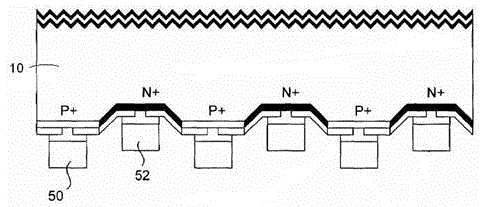
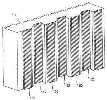
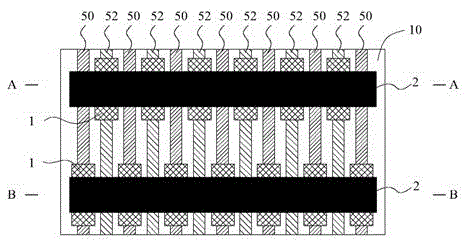
[0038] Such as Figure 6 As shown, the back-contact solar cell 10 of this implementation has a specification of 125X125mm produced by SUNPOWER Company of the United States, and it is necessary to cut out 18 battery chips with a specification of 32.4X20. There are 6 blocks vertically and vertically, leaving silicon chips on the left and right edges for use in other sizes, and the positive electrodes of the 3 blocks on the upper edge are drawn out, such as Figure 7 As shown, the positive terminal 5 of the back contact battery 10 itself can be used, and the negative terminal is that after the positive grid line 50 is covered by the insulating layer 1, the negative grid not covered by the insulating layer 1 is covered by the conductive layer 2 on the insulating layer 1. The line 52 is confluenced and conducted, and is drawn out from the negative poles of the three blocks below, such as Figure 9 As shown, the negative electrode terminal 6 of the back contact battery 10 itself ca...

Embodiment 2

[0044] In embodiment 1, if the conductive layer 2 is a non-solderable material, it can be as follows Figure 10 and Figure 11 As shown, the conductive solderable layer 3 is screen-printed on the soldering point on the conductive layer 2, and the electrode lead wires are welded on the solderable layer 3. If solderable copper paste is used as solderable layer 3 pad paste, use 0.06mm thick steel mesh screen printing, and the curing temperature is set to 140°C; if solderable silver paste is used as solderable layer 3 pad paste, use 0.06mm thick stencil screen printing, the curing temperature is set to 120°C; if low temperature solder paste is used as the solderable pad paste, 0.1mm thick stencil screen printing is used, cured by a reflow oven, and the central curing temperature is set to 160 °C.

Embodiment 3

[0046] Such as Figure 12 and Figure 13 As shown, in embodiment 1, the conductive profile of the copper strip 8 with the conductive adhesive layer 7 of 2 mm is used to replace the conductive layer 2, and the hot pressing process is used to bond the copper strip 8 with the conductive adhesive layer 7 to the prepared The back of the insulating layer 1 is in contact with the corresponding position of the lead-out area of ​​the positive and negative electrodes of each battery chip to be cut out on the battery 10, so as to form the positive and negative electrode confluence and lead-out electrode terminals of each battery chip.

[0047] The production process is as follows:

[0048] First place the back-contact battery 10 with the backlight facing up on the screen printing platform, and accurately align the alignment points of the grid line insulating coating screen and the back-contact battery 10, and then use the mask screen printing process to place the insulation The ink pas...


PUM


Abstract

The invention discloses an electrode extracting method for precisely processing back-contact-type solar cells into cell chips, and belongs to the technical field of solar cells. The electrode extracting method aims at precisely processing the efficient back-contact cells into the small chips with various sizes, achieving an electrode extracting manufacturing method and preventing short circuits caused by dislocation of adjacent grid lines. The electrode extracting method is mainly characterized by including the step that on the backlight surfaces of the back-contact-type cells, different-polarity grid lines cut into the positive electrode extraction ends and the negative electrode extraction ends of the chips are covered with insulating layers and grid line current-converging conductive layers for converging currents for conduction with the mask silk-screen printing technology. By means of the electrode extracting method, the percent of pass of the high-voltage-output chips is 99% or above, short circuits, caused by current converging position intersection errors of the electrode grid lines, between the adjacent grid lines are eliminated, and production cost is remarkably reduced accordingly.

Description

technical field [0001] The invention discloses an electrode lead-out method for processing various high-efficiency miniaturized battery chips with a high-efficiency back-contact solar cell, which belongs to the technical field of solar cells. Background technique [0002] At present, back-contact solar cells are widely used due to their high power generation efficiency, and researchers have continuously researched and developed many back-contact solar cells with different structures (hereinafter referred to as back-contact cells or batteries). The back contact cell refers to a silicon substrate solar cell in which the n+ electrode of the emitter region and the p+ electrode of the base region are located on the back of the silicon solar cell. Utilization rate and conversion efficiency; easy to assemble, the positive and negative electrodes are on the back, the components are packaged in a coplanar connection, the interval between the cells is reduced, the packaging density is...

Claims


Application Information

Patent Timeline
Patent Type & Authority Applications(China)
IPC IPC(8): H01L31/0224H01L31/18
CPCH01L31/0224H01L31/022441H01L31/18Y02E10/50Y02P70/50
Inventor 李毅李全相吴志武胡盛明孙坚
Owner SHEN ZHEN TRONY SCI & TECH DEV CO LTD
Why Eureka
Try Eureka