Test structure for monitoring source and drain polycrystalline silicon etching

A technology for testing structure and polysilicon, applied in semiconductor/solid-state device testing/measurement, electrical components, electrical solid-state devices, etc., can solve problems such as loss, etching residue, etc., and achieve the effect of reducing the risk of subsequent losses

Active Publication Date: 2012-05-30
SHANGHAI HUAHONG GRACE SEMICON MFG CORP
View PDF5 Cites 9 Cited by
  • Summary
  • Abstract
  • Description
  • Claims
  • Application Information

AI Technical Summary

Problems solved by technology

However, in the existing process of forming the source and drain regions with polysilicon, there is no effective method for monitoring the above-mentioned etching residues, and failures are often found in the product testing stage, and then the problem caused by the etching residues is found after failure analysis, resulting in risk of subsequent loss

Method used


Image

  • Test structure for monitoring source and drain polycrystalline silicon etching
  • Test structure for monitoring source and drain polycrystalline silicon etching
  • Test structure for monitoring source and drain polycrystalline silicon etching

Examples


Embodiment Construction

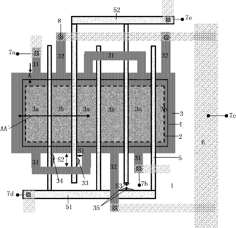
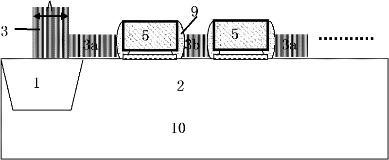
[0019] Such as figure 1 As shown, it is a schematic diagram of the layout of the test structure used to monitor the source-drain polysilicon etching according to the embodiment of the present invention; figure 2 shown, is figure 1 Schematic diagram of the cross-section of the AA` axis. The embodiment of the present invention is used to monitor the source-drain polysilicon etching test structure, which is formed on the scribe groove area of ​​the silicon substrate 10, and the active area 2 is isolated by the shallow trench isolation 1, including:

[0020] Multiple rows of gate polysilicon 5 are arranged in parallel on the active region 2 , and the long side direction of the gate polysilicon 5 is perpendicular to the long side direction of the active region 2 .

[0021] The source-drain polysilicon 3 covering the active region 2 and the gate polysilicon 5, the source-drain polysilicon 3 includes multiple rows of source-drain regions 3a, 3b arranged in parallel and a plurality...


PUM


Abstract

The invention discloses a test structure for monitoring source and drain polycrystalline silicon etching, comprising a plurality of columns of gate polycrystalline silicon arranged on an active region in parallel as well as source and drain polycrystalline silicon covered on the active region and the gate polycrystalline silicon, wherein the source and drain polycrystalline silicon arranged at two sides of the gate polycrystalline silicon forms source and drain regions; the source and drain regions in an odd column and an even column are respectively connected by using source and drain regionconnecting lines and are respectively led out to form a test port; and the gate polycrystalline silicon in an odd column and an even column is respectively connected by using a polycrystalline silicon gate connecting line and is respectively led out to form a test port. By using the test structure provided by the invention, the electric leakage problem caused by the residue of polycrystalline silicon obtained after the source and drain polycrystalline silicon is etched can be effectively monitored at the accept test stage of a silicon wafer, the fracture problem of the polycrystalline siliconobtained after the source and drain polycrystalline silicon is subjected to planarization etching can be effectively monitored, and risks for causing following loss can be reduced.

Description

technical field [0001] The invention relates to a monitoring and testing structure of a semiconductor integrated circuit manufacturing process, in particular to a testing structure for monitoring source and drain polysilicon etching. Background technique [0002] In the existing process of forming source and drain regions with polysilicon, the active area on the silicon wafer is isolated by shallow trench isolation, and the device includes a plurality of polysilicon gates formed on the active area and arranged in parallel. And the polysilicon gate is also covered with source and drain polysilicon, and the source and drain polysilicon is formed by first growing a layer of polysilicon on the surface of the entire silicon wafer on which the polysilicon gate is formed, and then etching the source and drain polysilicon; The source and drain polysilicon are separated by each of the polysilicon gates and form the source and drain regions of the device on both sides of each of the p...

Claims


Application Information

Patent Timeline
Patent Type & Authority Applications(China)
IPC IPC(8): H01L23/544H01L21/66
Inventor 金锋刘梅
Owner SHANGHAI HUAHONG GRACE SEMICON MFG CORP
Why Eureka
Try Eureka