

Solid-state imaging device and manufacturing method thereof, and electronic apparatus
A solid-state imaging device and solid-state imaging technology, which are used in electric solid-state devices, radiation control devices, televisions, etc., can solve the problems of impossible microfabrication, difficult to overlap the optical center Q of the viewing angle area, and difficult to focus, and reduce the number of lenses. Effect
Inactive Publication Date: 2012-05-30
SONY SEMICON SOLUTIONS CORP
View PDF5 Cites 29 Cited by
- Summary
- Abstract
- Description
- Claims
- Application Information
AI Technical Summary
Problems solved by technology
That is, when the semiconductor chip 167 is bent one by one, microfabrication is impossible, and the center P of the viewing angle area and the optical center Q of the lens are difficult to coincide with each other
Therefore, it is difficult to focus uniformly across the entire viewing angle area
Method used
View moreImage
Smart ImageViewing Examples

Examples
no. 1 example
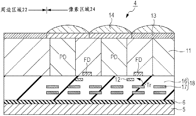
[0072] 1. First Embodiment (A structural example of a solid-state imaging device and an example of its manufacturing method)
[0073] 2. Second Embodiment (A structural example of a solid-state imaging device and an example of its manufacturing method)
no. 3 example
[0074] 3. Third Embodiment (A structural example of a solid-state imaging device and an example of its manufacturing method)
no. 4 example
[0075] 4. Fourth Embodiment (A structural example of a solid-state imaging device and an example of its manufacturing method)
Login to View More PUM
 Abstract
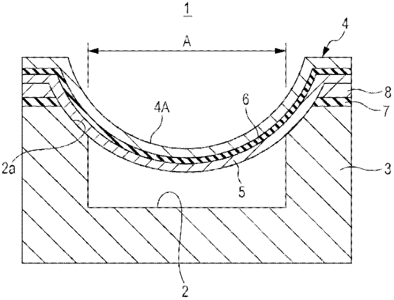
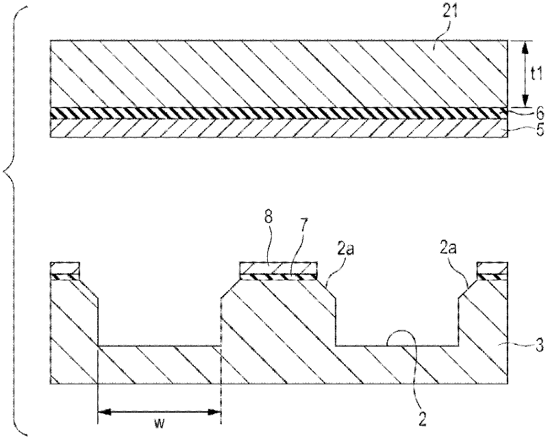
A solid-state imaging device (1) includes a supporting substrate (3) that includes a concave portion (2), a solid-state imaging chip (4) that is bonded on the supporting substrate (3) so as to seal the concave portion (2) in a view-angle region, a stress film (5) that is formed on the surface of the solid-state imaging chip (4), and an imaging surface curved toward the concave portion (2) at least in the view-angle region.
Description
[0001] Cross References to Related Applications [0002] The present application contains subject matter related to the disclosure of Japanese Priority Patent Application JP 2010-260973 filed in the Japan Patent Office on Nov. 24, 2010, the entire content of which is hereby incorporated by reference. technical field [0003] The present invention relates to a solid-state imaging device, a method of manufacturing the same, and an electronic device such as a camera including the solid-state imaging device. Background technique [0004] As a solid-state imaging device (imaging sensor), a CMOS solid-state imaging device, a CCD solid-state imaging device, and the like are known. Such as Figure 39 As shown, a camera 161 using a solid-state imaging device generally includes a solid-state imaging device 162 formed in a flat plate shape and an imaging lens system 164 composed of a plurality of lenses 163 . When an imaging lens system images an object, a focus position deviates betw...
Claims
Login to View More Application Information
Patent Timeline
 Patent Type & Authority Applications(China)
IPC IPC(8): H01L27/146H04N5/374H04N23/40
CPCH01L27/1464H01L2924/0002H01L27/1469H01L27/14634H01L23/13H01L27/14618H01L2924/00
Inventor 糸长总一郎
Owner SONY SEMICON SOLUTIONS CORP