
Signal acquisition device of memory bus

A signal acquisition and memory bus technology, applied in the field of high-performance computing, can solve the problems of low versatility, difficulty, high-speed oscilloscopes and logic analyzers, etc., to improve the acquisition effect, high input impedance, and reduce interference. Effect

Active Publication Date: 2014-11-26
INST OF COMPUTING TECH CHINESE ACAD OF SCI
View PDF3 Cites 0 Cited by
  • Summary
  • Abstract
  • Description
  • Claims
  • Application Information

AI Technical Summary

Problems solved by technology

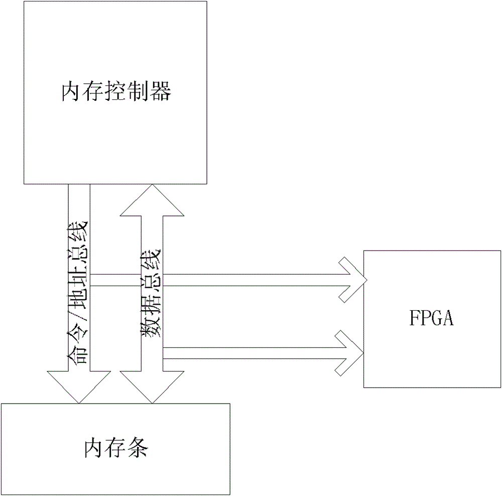
However, its shortcomings are also obvious: 1) The limited number of channels of the oscilloscope determines that it can only monitor certain bits in the 100-bit memory bus at the same time.
Although the logic analyzer can listen to signals with a width of hundreds of bits at the same time, it is difficult to find a position to fix its probe in a highly integrated motherboard in actual use, unless it is customized with its specific measurement interface (such as mid-bus) hardware
2) These two devices focus on collecting signals, but cannot effectively process the acquired information in real time, and their caches can only store data within a short time interval, and cannot continuously capture memory access information
3) High-speed oscilloscopes and logic analyzers are too expensive and not very versatile
The patent application with the application number US20060461567 discloses a system for monitoring the memory bus, but only some statistical information can be collected using counters

Method used


Image

  • Signal acquisition device of memory bus
  • Signal acquisition device of memory bus
  • Signal acquisition device of memory bus

Examples


Embodiment Construction

[0027] In order to make the object, technical solution and advantages of the present invention clearer, the present invention will be further described in detail below in conjunction with the accompanying drawings. It should be understood that the specific embodiments described here are only used to explain the present invention, not to limit the present invention.

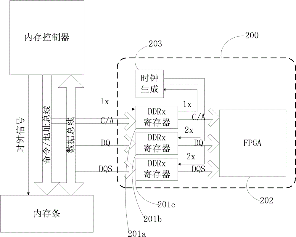
[0028] DDRx registers and memory buffers are two special chips currently used in server memory sticks, which are used to reduce the electrical load of the memory stick itself; among them: DDRx registers are used to produce RDIMM (Registered Dual In-line Memory Module, dual in-line memory module with registers) In-line memory module), which buffers and forwards the commands and address signals sent by the memory controller to the memory particles on the memory module; the memory buffer is used to produce LRDIMM (Load-Reduced Dual In-line Memory Module, low-load dual-row DDRx register), it can also buffer the bidire...


PUM


Abstract

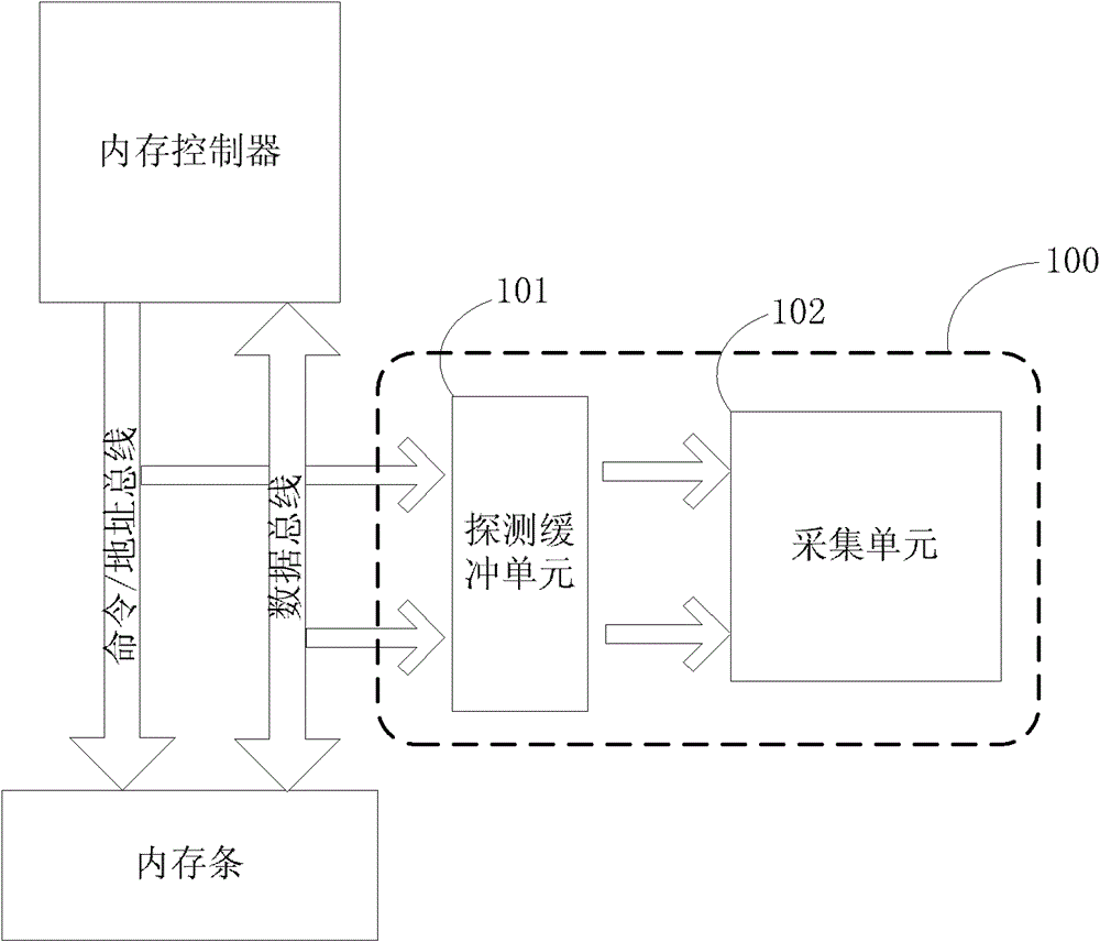
The invention provides a signal acquisition device of a memory bus, which comprises a detecting buffer unit and an acquisition unit, wherein the detecting buffer unit is suitable for acquiring signals of commands / an address bus and / or a data bus between a memory controller and memory chip and buffering and outputting the signals, and the acquisition unit is suitable or converting the buffered and output signals into data. By means of selection of input impedance of the detecting buffer unit, the signals of the memory bus are unaffected when signal acquisition is performed for the memory bus. The detecting buffer unit is a memory buffer or a DDRx register, and the acquisition unit is an FPGA (field programmable gate array), a high-speed oscilloscope or a logical analyzer. By the aid of the signal acquisition device, the problem of signal integrity when the FPGA performs signal acquisition for the memory bus is solved, so that a method for effectively acquiring memory signals can be carried out without interfering normal operation of an original memory system. Besides, the problem that caches of the high-speed oscilloscope and the logical analyzer can be only used for storing data at short time intervals is solved, so that the signals can be continuously acquired and outputted.

Description

technical field [0001] The invention relates to the fields of high-performance computing and signal acquisition, in particular to a signal acquisition device for a memory bus. Background technique [0002] Collecting memory bus signals is the basis for hardware to capture memory access information in real time. Acquisition of memory access information: it can help software designers improve memory access behavior and improve application software performance; it can help architecture designers find defects in existing memory systems, so as to improve them; it can also help hardware designers analyze memory protocols, Debug hardware. [0003] The memory bus includes a command bus, an address bus and a data bus, connecting the memory controller and memory particles, with a total width of about 100 bits. The existing memory bus acquisition methods are all bypass interception methods, where a certain place on the memory bus is selected as the acquisition point, and different de...

Claims


Application Information

Patent Timeline
Patent Type & Authority Patents(China)
IPC IPC(8): G06F13/16G06F11/34
Inventor 崔泽汉陈明宇包云岗朱晏张金勇
Owner INST OF COMPUTING TECH CHINESE ACAD OF SCI
Learn More