Semiconductor memory device for improving signal integrity issue and semiconductor system

A memory and semiconductor technology, applied in the direction of semiconductor devices, information storage, static memory, etc., can solve the problems of signal integrity reduction, difficult transmission, signal error, etc.

Inactive Publication Date: 2017-03-15
SAMSUNG ELECTRONICS CO LTD
View PDF5 Cites 3 Cited by
  • Summary
  • Abstract
  • Description
  • Claims
  • Application Information

AI Technical Summary

Problems solved by technology

Degradation of signal integrity makes it difficult to transfer signals quickly and causes errors during access operations including write operations and read operations of DRAM

Method used


Image

  • Semiconductor memory device for improving signal integrity issue and semiconductor system
  • Semiconductor memory device for improving signal integrity issue and semiconductor system
  • Semiconductor memory device for improving signal integrity issue and semiconductor system

Examples


Embodiment Construction

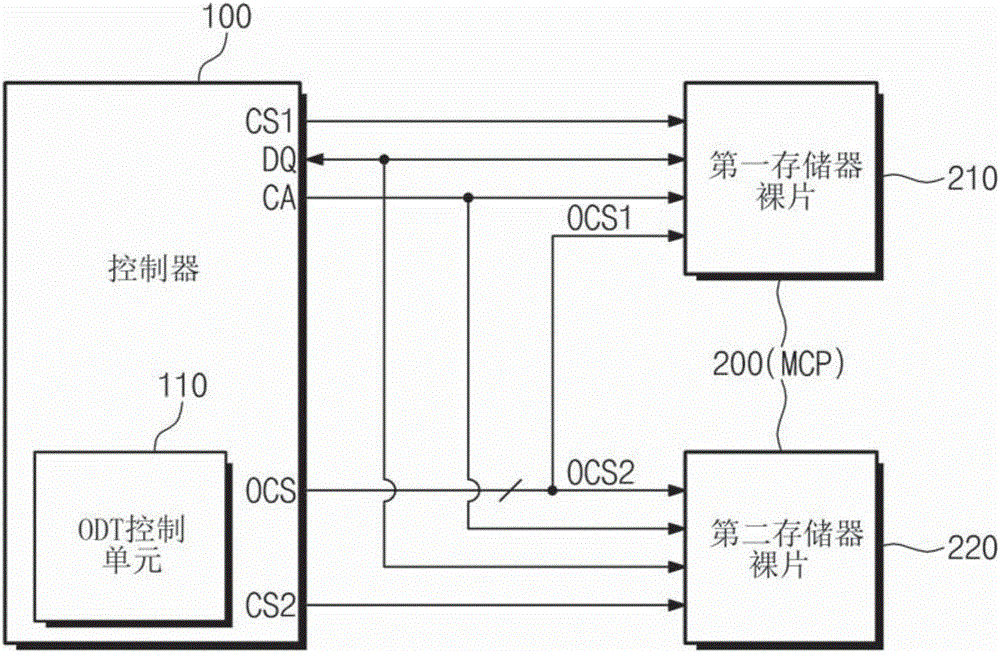
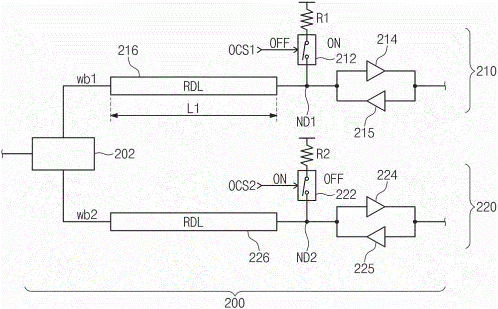
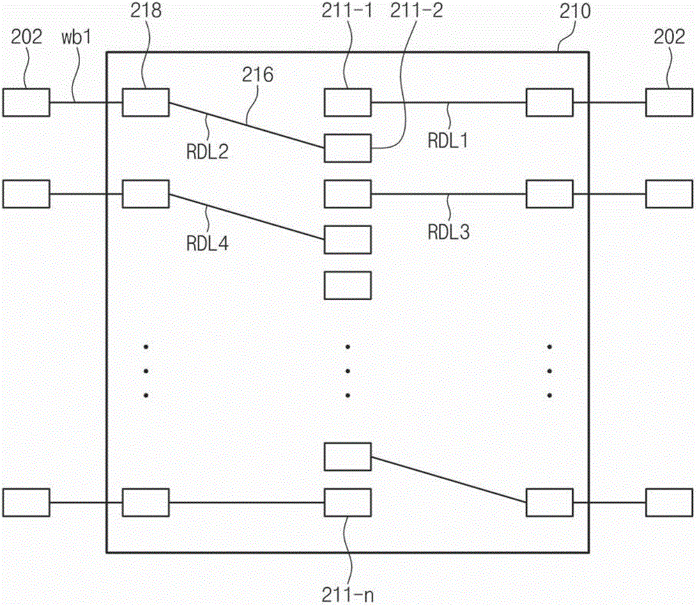
[0048] Various example embodiments will be described more fully hereinafter with reference to the accompanying drawings, in which some example embodiments are shown. Inventive concepts may, however, be embodied in many different forms and should not be construed as limited to the example embodiments set forth herein.

[0049] It will be understood that when an element or layer is referred to as being "on," "connected to," or "coupled to" another element or layer, it can be directly on the other element or layer. An element or layer may be on, connected to, or bonded directly to another element or layer, or intervening elements or layers may be present. In contrast, when an element or layer is referred to as being “directly on,” “directly connected to” or “directly coupled to” another element or layer, there are no intervening elements or layers present. Like reference numerals refer to like elements throughout. As used herein, the term "and / or" includes any and all combinati...


PUM


Abstract

The invention provides a semiconductor memory device for improving signal integrity issue and a semiconductor system. The semiconductor memory device includes a first memory die having a first termination resistor for an on-die termination and a second memory die having a second termination resistor for an on-die termination and formed on the first memory die. Each of the first and second memory dies has a center pad type and operates based on a multi-rank structure. When the first memory die is accessed, the second termination resistor is connected to the second memory die, and when the second memory die is accessed, the first termination resistor is connected to the first memory die.

Description

[0001] This application claims priority from Korean Patent Application No. 10-2015-0125715 filed with the Korean Intellectual Property Office on Sep. 4, 2015, the contents of which are hereby incorporated by reference in their entirety. technical field [0002] Some examples of the inventive concepts relate to semiconductor memory devices, and more particularly, to semiconductor memory devices of a stacked chip structure in which a plurality of memory dies are stacked. Background technique [0003] Dynamic Random Access Memory DRAM may be implemented in multi-chip packages to increase storage capacity. That is, a multi-chip package means a package in which a plurality of memory dies are stacked. For example, a plurality of memory dies may have a substrate interposed therebetween and may receive signals provided from a controller. For example, this structure may be called a dual-rank structure. [0004] As the transfer speed increases, the swing width of the signal exchange...

Claims


Application Information

Patent Timeline
Patent Type & Authority Applications(China)
IPC IPC(8): G11C5/02G11C5/06
CPCG11C5/02G11C5/06H01L2224/16145H01L2224/16225H01L2924/15192H01L2924/15311G11C7/1057G11C7/1084H01L28/00G11C11/4093H10B43/27H01L25/0657G11C11/4087G11C11/4096H01L2225/06513H01L2225/06544H10B12/50
Inventor 金京范文贤锺李稀裼车承勇
Owner SAMSUNG ELECTRONICS CO LTD
Why Eureka
Try Eureka