High-density PCB design method based on microstrip line far-end crosstalk
A technology of far-end crosstalk and design method, applied in the direction of computer design circuit, electrical components, printed circuit manufacturing, etc., can solve problems such as increasing PCB size, save space, improve PCB design success rate, and solve signal integrity problems. Effect
- Summary
- Abstract
- Description
- Claims
- Application Information
AI Technical Summary
Problems solved by technology
Method used
Image
Examples
Embodiment Construction
[0022] The present invention will be further described below in conjunction with accompanying drawing.
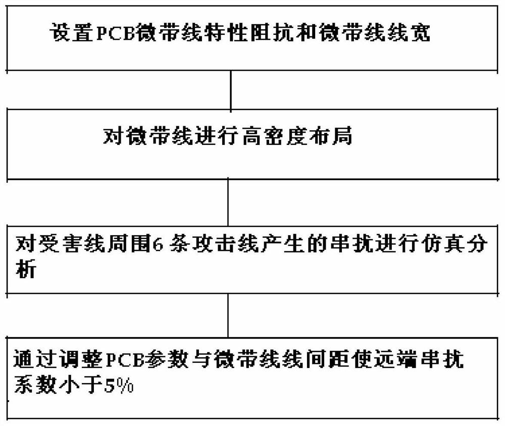
[0023] Such as figure 1 As shown, a high-density PCB board design method based on microstrip far-end crosstalk includes the following steps:
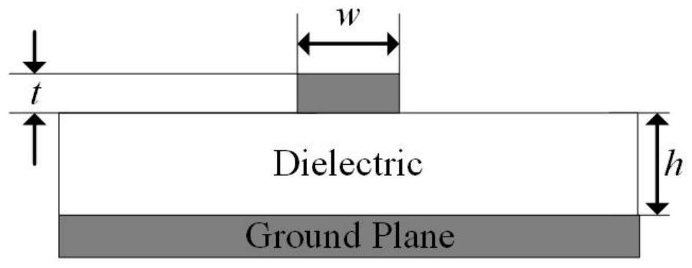
[0024] Step 1. Set the characteristic impedance of the PCB microstrip line and the line width of the microstrip line. First, select the PCB material made of copper clad material (FR4 material), then set the thickness of the microstrip line, and calculate the distance between the microstrip line and the ground layer , when the microstrip line is selected as the transmission model, the characteristic impedance Z of the microstrip line 0 Described by formula (1),
[0025]
[0026] In the formula, ε r Represents the relative permittivity of the PCB board, h represents the distance between the microstrip line and the ground, w represents the width of the microstrip line, and t represents the thickness of the microstrip line. Here, t...
PUM
 Abstract
Description
Claims
Application Information


