Supercharge Your Innovation With Domain-Expert AI Agents!

storage device

A storage device and storage layer technology, applied in information storage, static storage, digital storage information, etc., can solve the problems of difficult to manufacture reference storage cells, difficult to prepare reference storage cells, etc.

Inactive Publication Date: 2017-05-24
SONY SEMICON SOLUTIONS CORP
View PDF8 Cites 0 Cited by
  • Summary
  • Abstract
  • Description
  • Claims
  • Application Information

AI Technical Summary

Problems solved by technology

[0008] However, depending on the configuration and manufacturing method of the memory element, it is not easy to manufacture such a reference memory cell
Specifically, in the case of the same type of memory element as described in JP-A-2006-196537 and JP-A-2009-43757, the resistance value of the memory element varies non-linearly with the read voltage level , so it is difficult to fabricate reference memory cells corresponding to all read voltages

Method used


Image

  • storage device
  • storage device
  • storage device

Examples


no. 1 approach

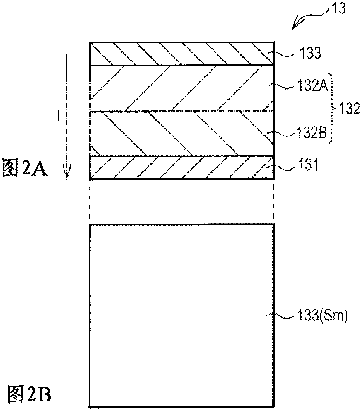
[0023] 1. First Embodiment (Example in which the area of ​​the second variable resistance element constituting the reference memory cell is larger than the area of ​​the first variable resistance element of the memory cell)

[0024] 2. Second Embodiment (Example in which the second variable resistance element constituting the reference memory cell is provided with a plurality of variable resistance elements having the same configuration as the first variable resistance element)

[0025]

[0026] [Configuration of Storage Device 1]

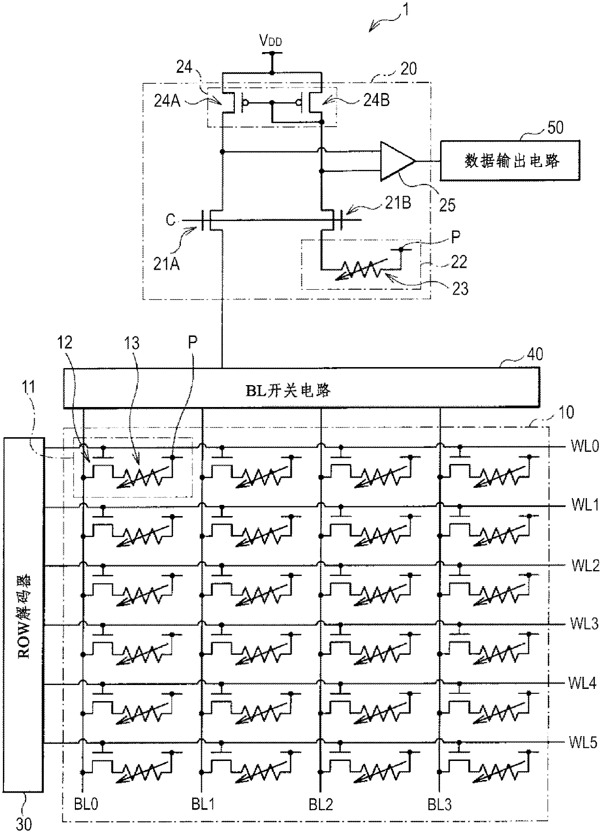
[0027] figure 1 A schematic configuration of the storage device 1 according to the first embodiment of the present invention is shown. This storage device 1 includes a memory array (storage unit) 10 , a readout circuit 20 , a ROW decoder 30 , a BL switch circuit 40 , and a data output circuit 50 .

[0028] (storage array 10)

[0029] The memory array 10 has a plurality of memory cells 11 arranged in a matrix (for example, 4 columns×6 rows) in ...

no. 2 approach

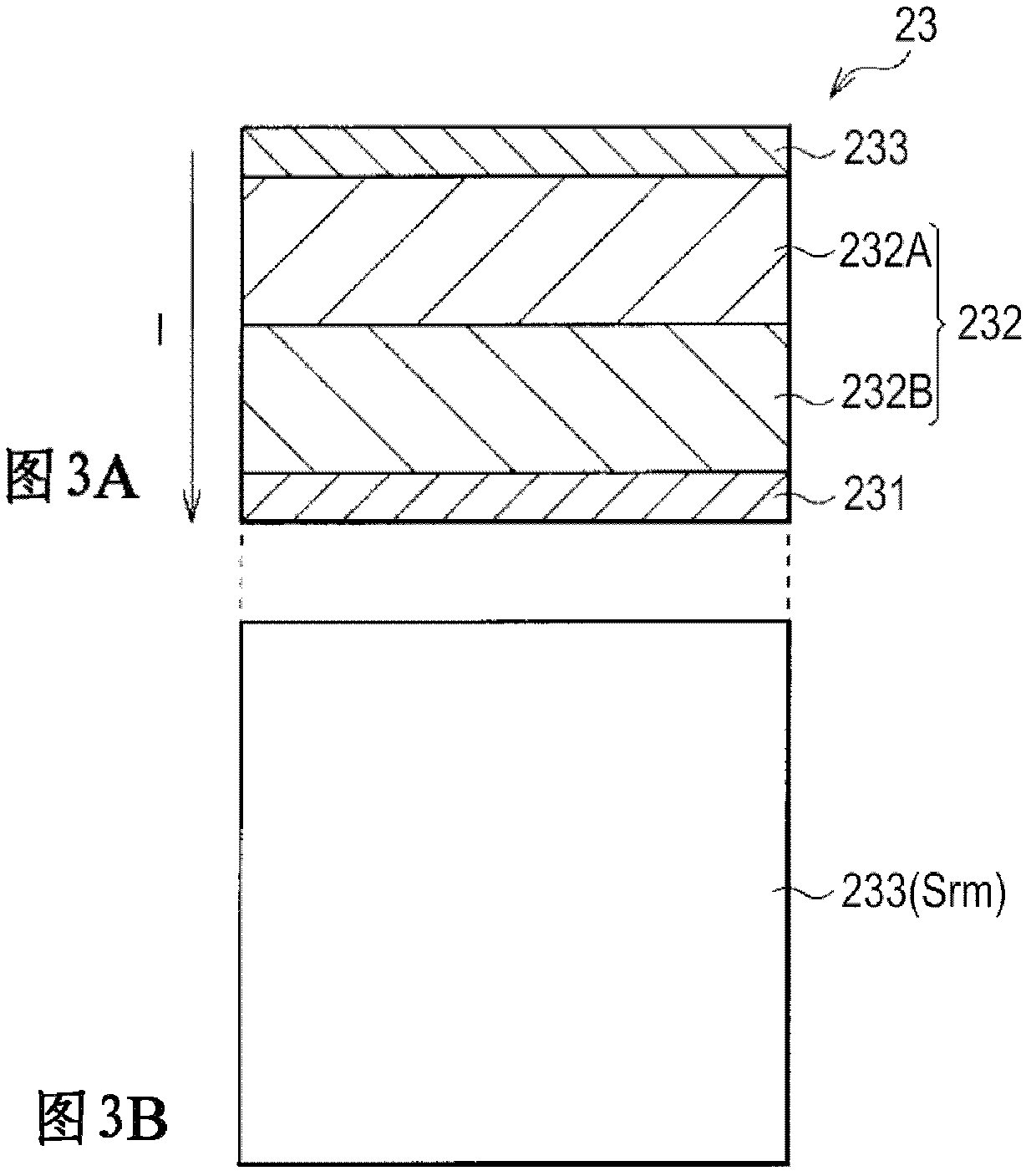
[0073] Figure 7 A schematic configuration of a storage device 2 according to a second embodiment of the present invention is shown. This embodiment differs from the first embodiment described above in that a plurality of variable resistance elements 26 having the same configuration as the variable resistance elements 13 in the memory cell 11 are included in the reference memory cell 22A as second variable resistance elements. Each of the plurality of variable resistance elements 26 is connected in parallel to one terminal of the transistor 21B for applying a read voltage through a transistor 27 . exist Figure 7 In this example, three variable resistance elements 26 are connected in parallel, but the number of variable resistance elements 26 may be two or more.

[0074] Figure 8A represents the cross-sectional configuration of the resistance change element 26, while Figure 8B A planar arrangement of the variable resistance element 26 is shown. The variable resistance e...


PUM


Abstract

A memory device comprising: a plurality of memory cells each including a first resistance change element; and a readout circuit which compares the resistance state of a memory cell selected from the plurality of memory cells with that of a reference memory cell resistance state, to determine the magnitude of the resistance value of the first variable resistance element; wherein, the reference storage unit includes a second variable resistance element, and the resistance value of the second variable resistance element relative to the applied voltage is smaller than that of the first variable resistance element at The resistance value in the high resistance state, and the second resistance change element exhibits the same resistance change characteristics as the first resistance change element. The present invention can accurately determine the resistance value of the memory cell, that is, determine whether the state is a writing state or an erasing state regardless of the reading voltage level.

Description

[0001] Cross References to Related Applications [0002] This application contains subject matter related to and claims priority from Japanese Patent Application JP 2010-276748 filed in the Japan Patent Office on Dec. 13, 2010, the entire content of which is hereby incorporated by reference. technical field [0003] The present invention relates to a memory device having a variable resistance memory element (variable resistance element), and more particularly, to a memory device provided with a readout circuit for determining a memory state (resistance value) from a reference memory cell. Background technique [0004] At present, non-volatile memory elements that do not erase information even when the power is turned off have been proposed, such as flash memory, ferroelectric random access memory (FeRAM), magnetoresistive random access memory (MRAM), and the like. In these memory elements, written information can be continuously held for a long time even when power is not su...

Claims


Application Information

Patent Timeline
Patent Type & Authority Patents(China)
IPC IPC(8): G11C13/00H10N99/00
CPCG11C11/5614G11C13/0011G11C13/004G11C2013/0042H10N70/245H10N70/882H10N70/8833H10N70/826H10B63/00G11C13/0069
Inventor 対马朋人北川真椎本恒则中岛智恵子吉原宏小方宪太郎
Owner SONY SEMICON SOLUTIONS CORP
Features
  • R&D
  • Intellectual Property
  • Life Sciences
  • Materials
  • Tech Scout
  • Unparalleled Data Quality
  • Higher Quality Content
  • 60% Fewer Hallucinations
Learn More