Flash memory chip and testing method thereof

A technology of flash memory chips and testing methods, applied in information storage, static memory, read-only memory, etc., can solve the problems of increasing the time of parallel testing, etc., and achieve the effect of reducing testing time and reducing testing waiting time

Active Publication Date: 2015-01-07
GIGADEVICE SEMICON (BEIJING) INC
View PDF7 Cites 0 Cited by
  • Summary
  • Abstract
  • Description
  • Claims
  • Application Information

AI Technical Summary

Problems solved by technology

Because the time for each chip to complete the operation instruction is different, for example, the first chip completes in 4s, and the rest of the chips complete in 6s, then the ATE will issue the second instruction after 6s, and the first chip will It is necessary to wait for 2 seconds before performing the second operation. If the completion time of each chip during the second operation is the same as that of the first operation, the first chip needs to wait again, and so on. several waits, which increases the time for parallel testing

Method used


Image

  • Flash memory chip and testing method thereof
  • Flash memory chip and testing method thereof
  • Flash memory chip and testing method thereof

Examples


Embodiment 1

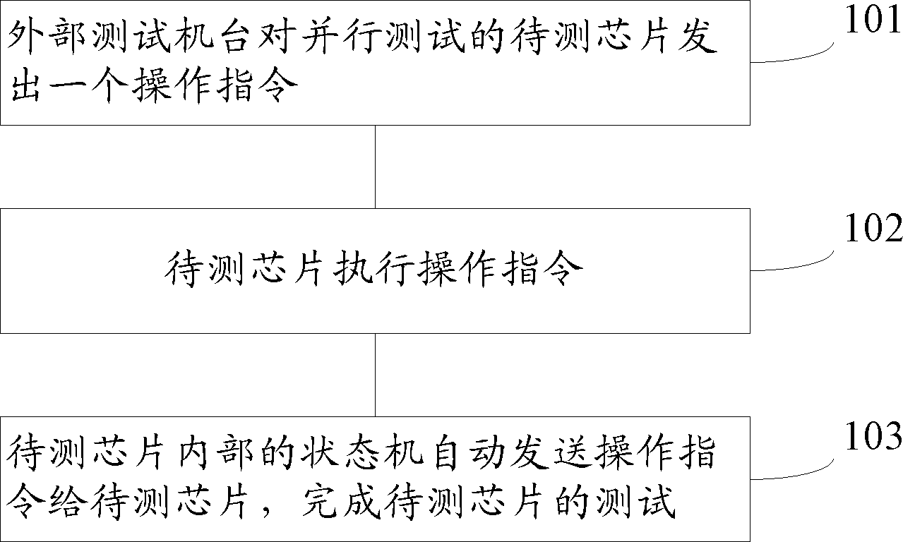
[0024] Please refer to figure 1 , showing a first embodiment of a method for testing a flash memory chip of the present invention, comprising the following steps:

[0025] Step 101, the external testing machine sends an operation instruction to the chips under test for parallel testing.

[0026] The external test machine sends an operation command to all the chips to be tested that need to be tested in parallel. The operation command here can be an operation command for logical function testing. For example, the external test machine operates the CKB of the chip to be tested: to the storage unit (cell ) erase operation instructions, program and verify operation instructions on memory cells that have been erased, and the like.

[0027] Step 102, the chip under test executes an operation instruction.

[0028] All the chips under test perform operations according to the operation instructions of the external test machine.

[0029] Step 103 , the state machine inside the chip t...

Embodiment 2

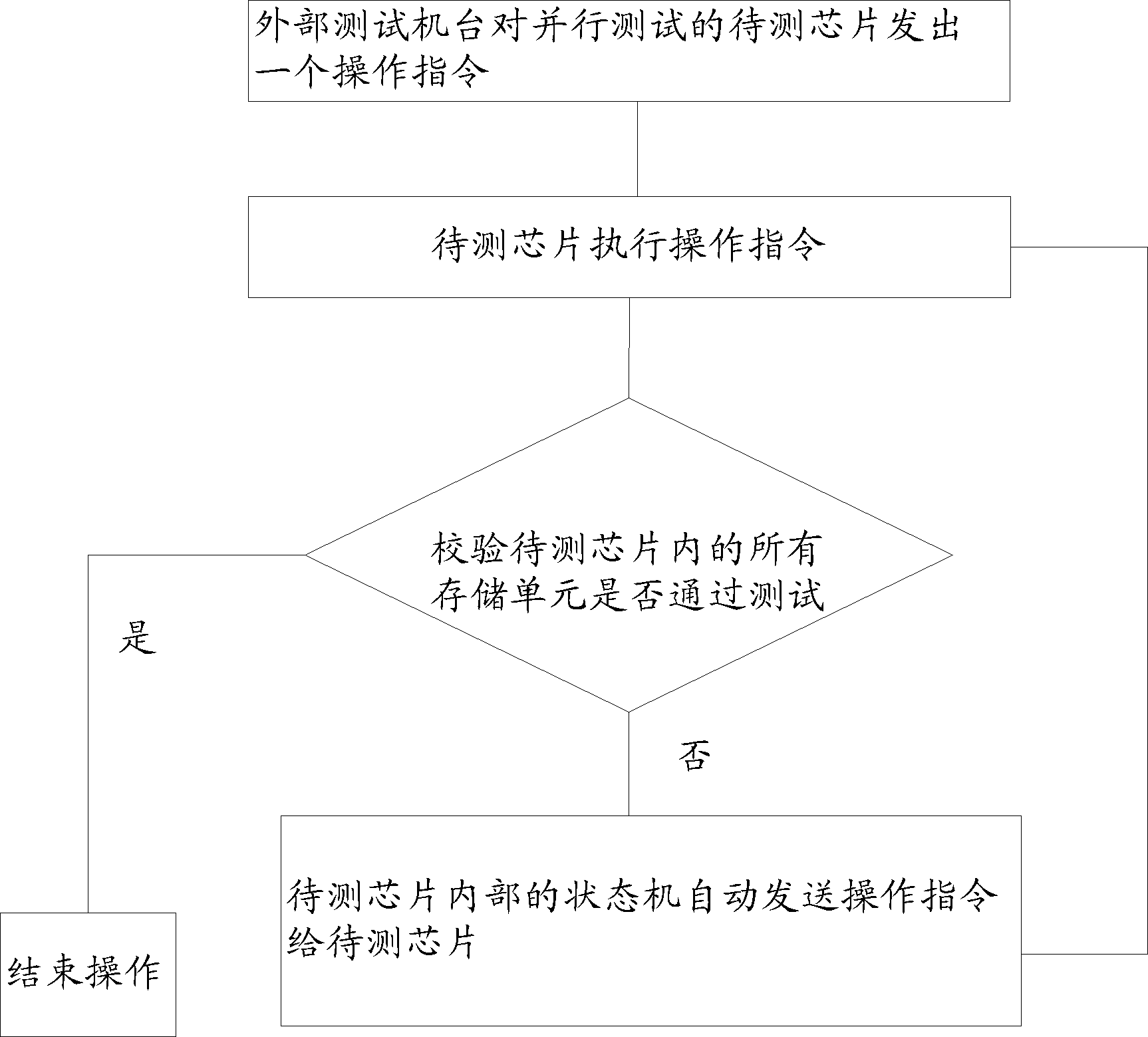
[0031] refer to figure 2 , showing a second embodiment of a method for testing a flash memory chip of the present invention, comprising the following steps:

[0032] In step 201, the external testing machine sends an operation command to the chips under test for parallel testing.

[0033] In step 202, the chip under test executes an operation instruction.

[0034] Step 203, check whether all storage units in the chip under test pass the test, if so, proceed to step 204; otherwise, the state machine inside the chip under test automatically sends an operation command to the chip under test, and returns to step 202.

[0035] Step 204, the state machine returns the test pass information to the external test machine.

[0036] By judging the execution results of the chip to be tested, whether all the storage units in the chip have completed the operation command, if yes, no operation is required, if not, it is necessary to issue an operation command to the chip to be tested, and ...


PUM


Abstract

The invention provides a testing method of a flash memory chip, which comprises the following steps of: sending an operation instruction to chips to be tested in parallel by an external test bench; executing the operation instruction by the chips to be tested; and automatically sending the operation instruction to each chip to be tested by a state machine inside each chip to be tested and finishing the testing of the chips to be tested. According the testing method of the flash memory chip, the time of parallel test can be shortened. The invention further provides the flash memory chip.

Description

technical field [0001] The invention relates to the technical field of semiconductor memory, in particular to a method for testing a flash memory chip and the flash memory chip. Background technique [0002] In order to verify the correctness of memory products, a series of testing procedures will be carried out before the products leave the factory. These storage products may include non-volatile memory products (for example, flash memory Flash Memory, or EEPROM, etc.), and may also include one-time programmable OTP memory. The general test process can include product pin (pin) short circuit / open circuit test, logic function test, electrical erasing characteristic test (to determine whether the data in the volatile memory can be electrically erased and rewritten with new data) , program code test (read the program code written into the non-volatile memory and compare it with the written program code to determine whether the read-write action of the non-volatile memory is c...

Claims


Application Information

Patent Timeline
Patent Type & Authority Patents(China)
IPC IPC(8): G11C29/08G11C16/02
Inventor 苏志强舒清明
Owner GIGADEVICE SEMICON (BEIJING) INC
Why Eureka
Try Eureka