A kind of semiconductor structure and its manufacturing method

A manufacturing method and semiconductor technology, applied in semiconductor/solid-state device manufacturing, semiconductor devices, electric solid-state devices, etc., can solve problems such as large leakage current

Active Publication Date: 2016-09-28
BEIJING YANDONG MICROELECTRONICS
View PDF7 Cites 0 Cited by
  • Summary
  • Abstract
  • Description
  • Claims
  • Application Information

AI Technical Summary

Problems solved by technology

Applying this method can effectively solve the problem of excessive leakage current due to the amplification effect of parasitic BJT when using NMOS / PMOS or CascadedNMOS / PMOS as ESD protection in thick epitaxial devices

Method used


Image

  • A kind of semiconductor structure and its manufacturing method
  • A kind of semiconductor structure and its manufacturing method
  • A kind of semiconductor structure and its manufacturing method

Examples


Embodiment Construction

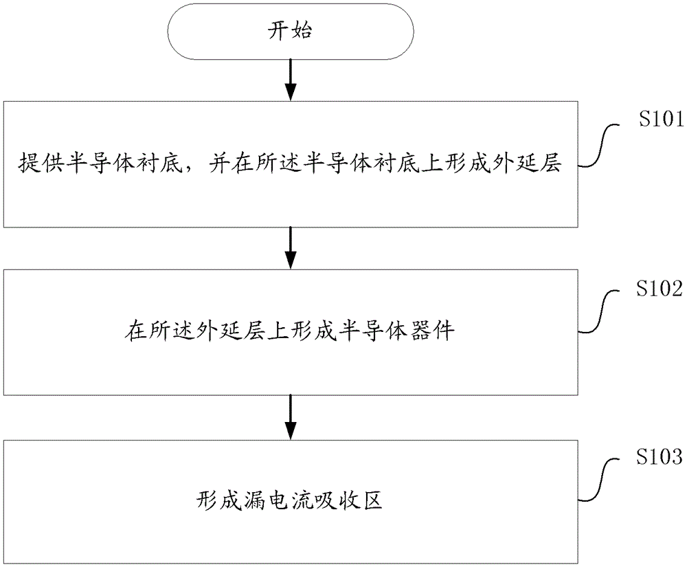
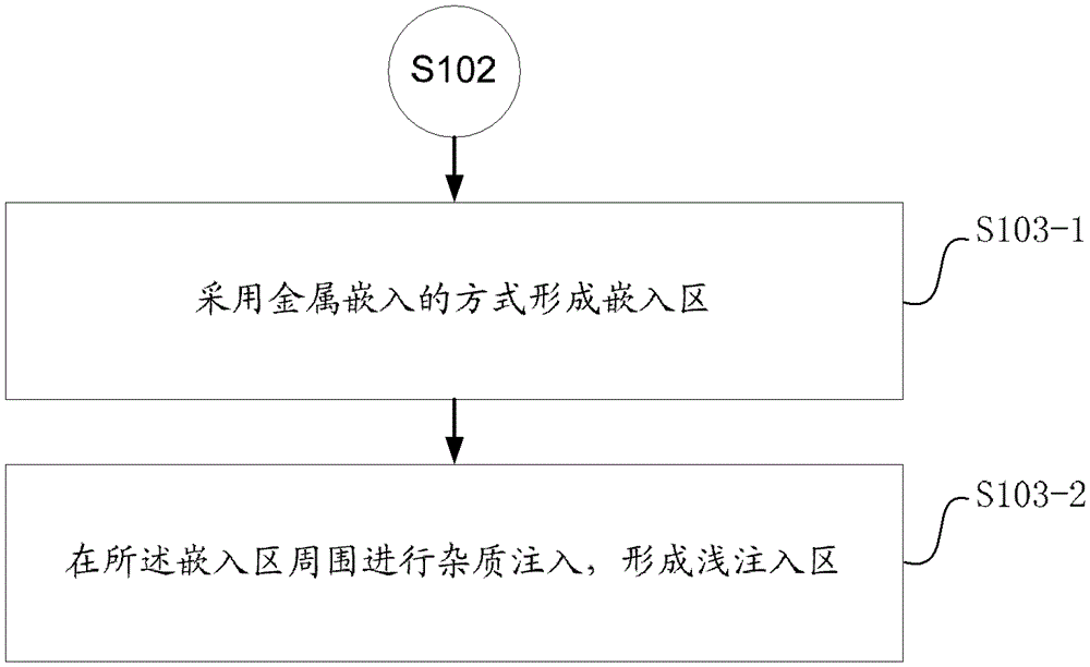
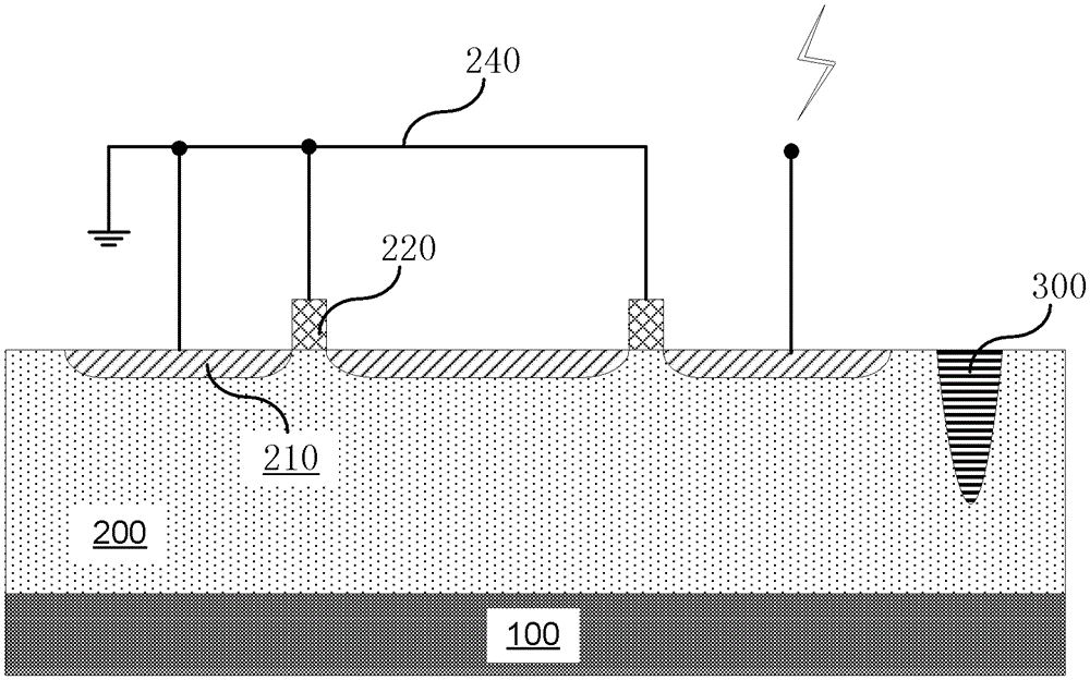
[0030] In order to make the object, technical solution and advantages of the present invention clearer, the embodiments of the present invention will be described in detail below with reference to the accompanying drawings.

[0031] Embodiments of the present invention are described in detail below, examples of which are shown in the drawings, wherein the same or similar reference numerals designate the same or similar elements or elements having the same or similar functions throughout. The embodiments described below by referring to the figures are exemplary only for explaining the present invention and should not be construed as limiting the present invention.

[0032] The following disclosure provides many different embodiments or examples for implementing different structures of the present invention. To simplify the disclosure of the present invention, components and arrangements of specific examples are described below. Of course, they are only examples and are not int...


PUM


Abstract

The invention provides a method for manufacturing a semiconductor structure, comprising the following steps: providing a semiconductor substrate, and forming an epitaxial layer on the semiconductor substrate; forming a semiconductor device on the epitaxial layer; forming a leakage current absorption region, the The leakage current absorbing region is located at one side of the drain region of the semiconductor device and is not in contact with the drain region. Correspondingly, the present invention also provides a semiconductor structure manufactured by applying the method. The method and the semiconductor structure of the invention can effectively reduce the leakage current in the thick epitaxial device, and further improve the overall performance of the semiconductor device.

Description

technical field [0001] The invention relates to the field of semiconductor manufacturing, in particular to a semiconductor structure and a manufacturing method thereof. Background technique [0002] Static electricity exists all the time in nature. When the human body can feel the existence of static electricity, the static electricity generated has reached tens of thousands of volts, which is enough to damage most electronic components. [0003] With the development of the semiconductor industry, integrated circuits with higher performance and stronger functions require greater component density, and the size, size, and space of each component, between components, or each component itself need to be further reduced (currently, it has reached nanometers. level), so the requirements for process control in the manufacturing process of semiconductor devices are relatively high. [0004] However, when the external environment of the chip or the static charge accumulated inside ...

Claims


Application Information

Patent Timeline
Patent Type & Authority Patents(China)
IPC IPC(8): H01L21/336H01L27/02H01L29/78
Inventor 姜一波曾传滨杜寰
Owner BEIJING YANDONG MICROELECTRONICS
Why Eureka
Try Eureka