Verifying method and verifying device for electrostatic protection of chip

A technology for electrostatic protection and verification devices, which is applied in the direction of electrical digital data processing, special data processing applications, instruments, etc., can solve problems such as heavy workload, affecting completeness and accuracy, and achieve improved reliability, strong completeness, Ease of use

Active Publication Date: 2012-08-29
FOSHAN SYNWIT TECH
View PDF3 Cites 9 Cited by
  • Summary
  • Abstract
  • Description
  • Claims
  • Application Information

AI Technical Summary

Problems solved by technology

It can be seen from the figure that if the number of pins reaches 40, then at least 1560 static charge discharge paths need to be checked, which is a lot of work and will affect completeness and accuracy

Method used


Image

  • Verifying method and verifying device for electrostatic protection of chip
  • Verifying method and verifying device for electrostatic protection of chip
  • Verifying method and verifying device for electrostatic protection of chip

Examples


Embodiment Construction

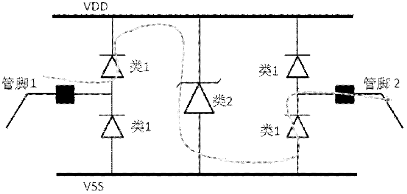
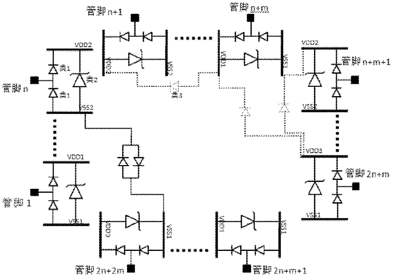
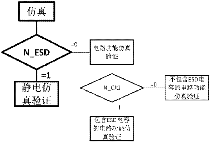
[0013] A verification method for chip electrostatic protection and a verification device provided by the present invention will be described in detail below with reference to the accompanying drawings and specific embodiments. At the same time, it is explained here that in order to make the embodiments more detailed, the following embodiments are the best and preferred embodiments, and those skilled in the art can also adopt other alternative ways to implement for some known technologies; and the accompanying drawings It is only for more specific description of the embodiments, but not intended to specifically limit the present invention.

[0014] The present invention covers any alternatives, modifications, equivalent methods and schemes made on the spirit and scope of the present invention. In order to provide the public with a thorough understanding of the present invention, specific details are set forth in the following preferred embodiments of the present invention, but ...


PUM


Abstract

The invention provides a verifying device and a verifying method for the electrostatic protection of a chip. In a network structure, the verifying device comprises a plurality of electrostatic protection verifying subunits, multiple groups of power supply ends and multiple groups of unit grounding ends; in a network, the verifying device comprises first-type electrostatic protecting apparatuses, a second-type electrostatic protecting apparatus and a third-type electrostatic protecting apparatus; each electrostatic protection verifying subunit comprises two first-type electrostatic protecting apparatuses and one second-type electrostatic protecting apparatus; the two first-type electrostatic protecting apparatuses are connected in series and then are connected with the second-type electrostatic protecting apparatus in parallel, wherein in a parallel structure, a cathode of one first-type electrostatic protecting apparatus and one end of the second-type electrostatic protecting apparatus are respectively connected with a power supply; an anode of the other first-type electrostatic protecting apparatus and the other end of the second-type electrostatic protecting apparatus are respectively connected with the ground; and one third-type electrostatic protecting apparatus is arranged between the power supply ends of any two electrostatic protection verifying subunits in a series direction.

Description

technical field [0001] The present invention relates to an electrostatic protection verification technology, more specifically, to a chip electrostatic protection verification method based on a diode network and a verification device thereof. Background technique [0002] Electrostatic discharge (ESD) accounts for a considerable proportion of circuit failures in the integrated circuit industry. With the increase of circuit integration, the thinning of gate oxide thickness, the application of multi-power and mixed-signal modules in complex circuits, larger Chip parasitic capacitance and higher operating frequency will make advanced devices and circuits more sensitive to ESD. In other words, electrostatic protection (ESD) is a key step in the design of all semiconductor chips, which determines the reliability and service life of the chip. As the complexity of the chip increases, the output pins of the chip also increase, which further increases the difficulty of electrostatic...

Claims


Application Information

Patent Timeline
Patent Type & Authority Applications(China)
IPC IPC(8): G06F17/50
Inventor 韩智毅张炜
Owner FOSHAN SYNWIT TECH
Why Eureka
Try Eureka