Welding process of non-contact intelligent card antenna

A non-contact smart card, welding process technology, applied in welding equipment, auxiliary welding equipment, welding/cutting auxiliary equipment, etc., can solve the problems of easy to touch the chip, difficult to ensure the accurate position of the antenna, manually dialing the chip and other problems. The effect of improving stability

Inactive Publication Date: 2012-09-05
ESIM TECH LTD
View PDF6 Cites 2 Cited by
  • Summary
  • Abstract
  • Description
  • Claims
  • Application Information

AI Technical Summary

Problems solved by technology

[0003] In the traditional process, when the antenna crosses over the chip and goes online, it is easy to touch the chip and change the position of the chip. It is difficult to ensure the accurate position of the antenna in the chip welding area, and the welding quality is not easy to control. Chips have a higher chance of

Method used


Image

  • Welding process of non-contact intelligent card antenna
  • Welding process of non-contact intelligent card antenna
  • Welding process of non-contact intelligent card antenna

Examples


Embodiment 1

[0038] A non-contact smart card antenna welding process, which includes the following sequential steps:

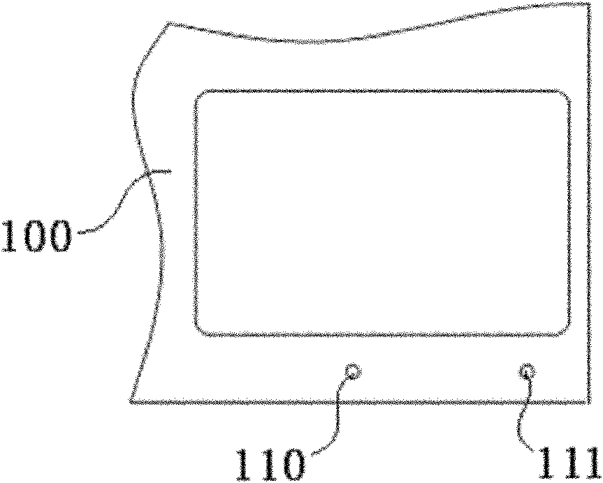
[0039] (1) see figure 1 . Two positioning holes 110, 111 for positioning in the X and Y directions are punched out on a single-layer card base material 100. The positioning holes 110 are used for the positioning of each material during the processing of each process. Of course, it can also be carried out directly with the edge of the material The positioning of each process or stamping any other positioning structures known to those skilled in the art.

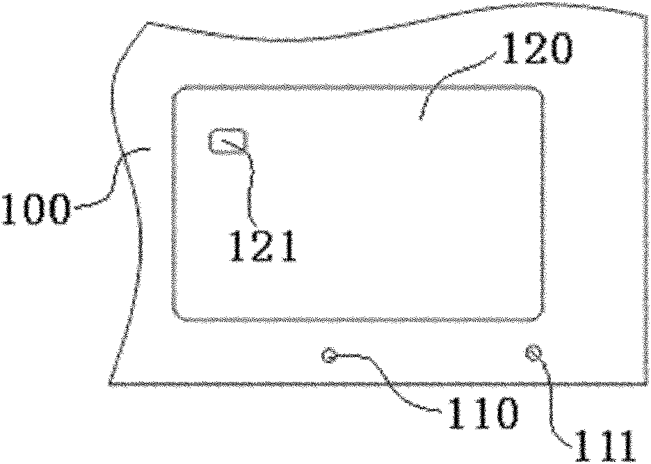
[0040] (2) see figure 2 , punch out a chip hole 121 in the card region 120 of a single-layer card base material 100; the chip hole 121 is a through hole.

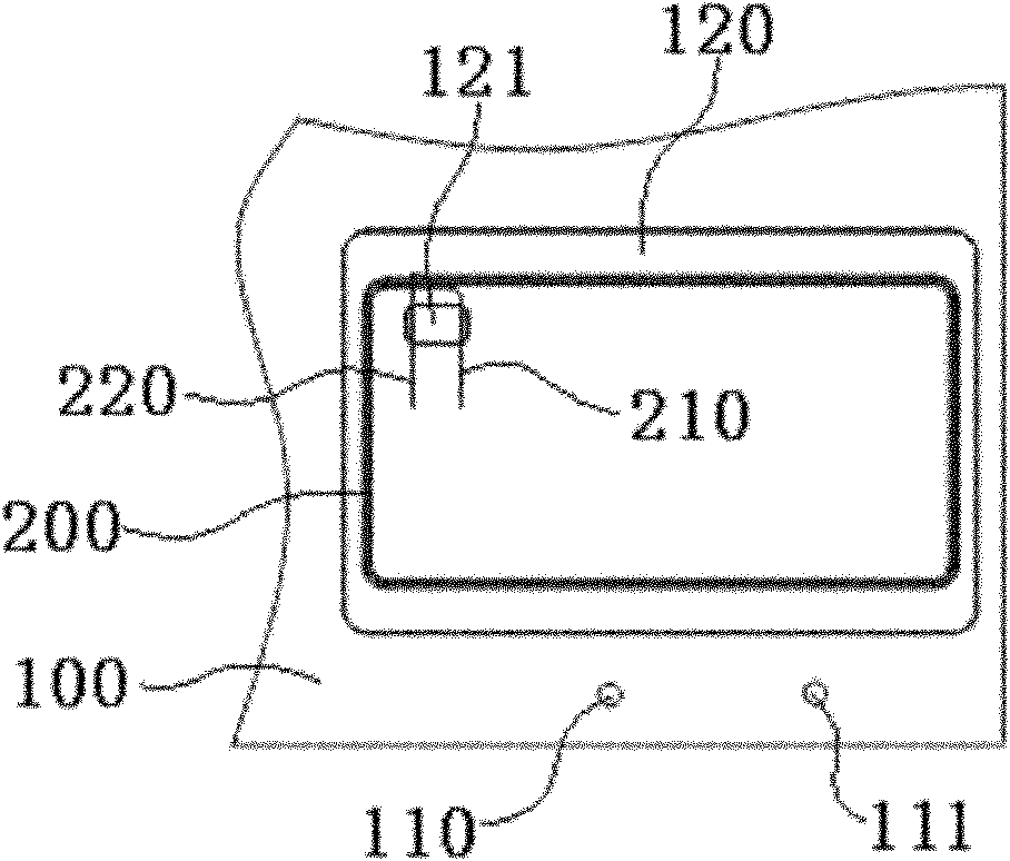
[0041] (3) see image 3 , bury the antenna 200 on the front surface of the card area 120 of the single-layer card base material 100, and the two welding ends 210, 220 of the antenna 200 straddle the chip hole 121;

[0042] (4) see Figure 4 , the chip 300 is fill...

Embodiment 2

[0045] The steps of this embodiment are the same as in Example 1, see Figure 7 , but in step (4), the black glue part 310 of the chip 300 faces the back of the card area 120 .

Embodiment 3

[0047] A non-contact smart card antenna welding process, which includes the following sequential steps:

[0048] (1) see Figure 8 , two positioning holes 110a, 111a for positioning in the X and Y directions are respectively punched on the single-layer card base material 100a, see Figure 9 Two positioning holes 100b, 111b for positioning in the X and Y directions are respectively punched on the single-layer card base material 100b. The positioning holes 110a, 111a, 100b, and 111b are used for the positioning of each material during the processing of each process. Directly use the edge to carry out the positioning of each process or punch any other positioning structures known to those skilled in the art.

[0049] (2) see Figure 10 with Figure 11 , chip holes 121a, 121b are respectively punched out in the card areas 120a, 120b of the two single-layer card base materials 100a, 100b; and single-layer upline card base material B

[0050] (3) see Figure 12 , bury the ante...


PUM


Abstract

The invention discloses a welding process of a non-contact intelligent card antenna. The welding process comprises the following sequential steps of: (1) a step of punching a chip hole in a single-layer card substrate; (2) a step of burying the antenna on the single-layer card substrate, wherein in the step, the antenna is buried in the first face of the single-layer card substrate and two welding ends of the antenna span across the chip hole; (3) a step of filling a chip into the chip hole, wherein the second face side of the single-layer card substrate, which corresponds to the first face, is filled into the chip hole in the step; and (4) a step of welding the antenna with the chip. According to the invention, the welding process improves the problems in the traditional process that the chip is moved easily when a wire spans across above the chip so that relative positions of the chip and the antenna are changed, the antenna cannot be ensured to be at a central position of a chip welding region, and a module needs to be usually moved manually and the antenna needs to be pulled, so that the production efficiency and the stability of the welding quality are improved.

Description

technical field [0001] The invention relates to the technical field of non-contact card preparation, in particular to a non-contact smart card antenna welding process. Background technique [0002] The current common non-contact card antenna and chip welding process, single-layer card base material punching (place chip hole) --- fill the chip --- bury the antenna on the card base material, and the antenna crosses the top of the chip welding area --- - Antenna and chip soldering. [0003] In the traditional process, when the antenna crosses over the chip and goes online, it is easy to touch the chip and change the position of the chip. It is difficult to ensure the accurate position of the antenna in the chip welding area, and the welding quality is not easy to control. Chips are more likely. Contents of the invention [0004] The technical problem to be solved by the present invention is to provide a non-contact smart card antenna welding process for the above-mentioned ...

Claims


Application Information

Patent Timeline
Patent Type & Authority Applications(China)
IPC IPC(8): B23K37/04H01R43/02H01Q1/22
Inventor 王峻峰张耀华王莉萍王建
Owner ESIM TECH LTD
Why Eureka
Try Eureka