
Pixel structure and corresponding liquid crystal display device

A technology of liquid crystal display device and pixel structure, which is applied in the direction of optics, instruments, electrical components, etc., can solve the problems of low aperture ratio and poor manufacturing stability of liquid crystal display devices, achieve good manufacturing stability, increase aperture ratio, and solve the problem of aperture ratio low effect

Inactive Publication Date: 2012-09-19
TCL CHINA STAR OPTOELECTRONICS TECH CO LTD
View PDF4 Cites 2 Cited by
  • Summary
  • Abstract
  • Description
  • Claims
  • Application Information

AI Technical Summary

Problems solved by technology

[0007] The object of the present invention is to provide a novel pixel structure and a corresponding liquid crystal display device, the pixel structure has a high aperture ratio and good manufacturing stability, so as to solve the problem of the low aperture ratio or stable manufacturing of the existing pixel structure and the corresponding liquid crystal display device. Poor technical issues

Method used


Image

  • Pixel structure and corresponding liquid crystal display device
  • Pixel structure and corresponding liquid crystal display device
  • Pixel structure and corresponding liquid crystal display device

Examples


Embodiment Construction

[0025] The following descriptions of the various embodiments refer to the accompanying drawings to illustrate specific embodiments in which the present invention can be practiced. The directional terms mentioned in the present invention, such as "up", "down", "front", "back", "left", "right", "inside", "outside", "side", etc., are for reference only The orientation of the attached schema. Therefore, the directional terms used are used to illustrate and understand the present invention, but not to limit the present invention.

[0026] In the figures, structurally similar units are denoted by the same reference numerals.

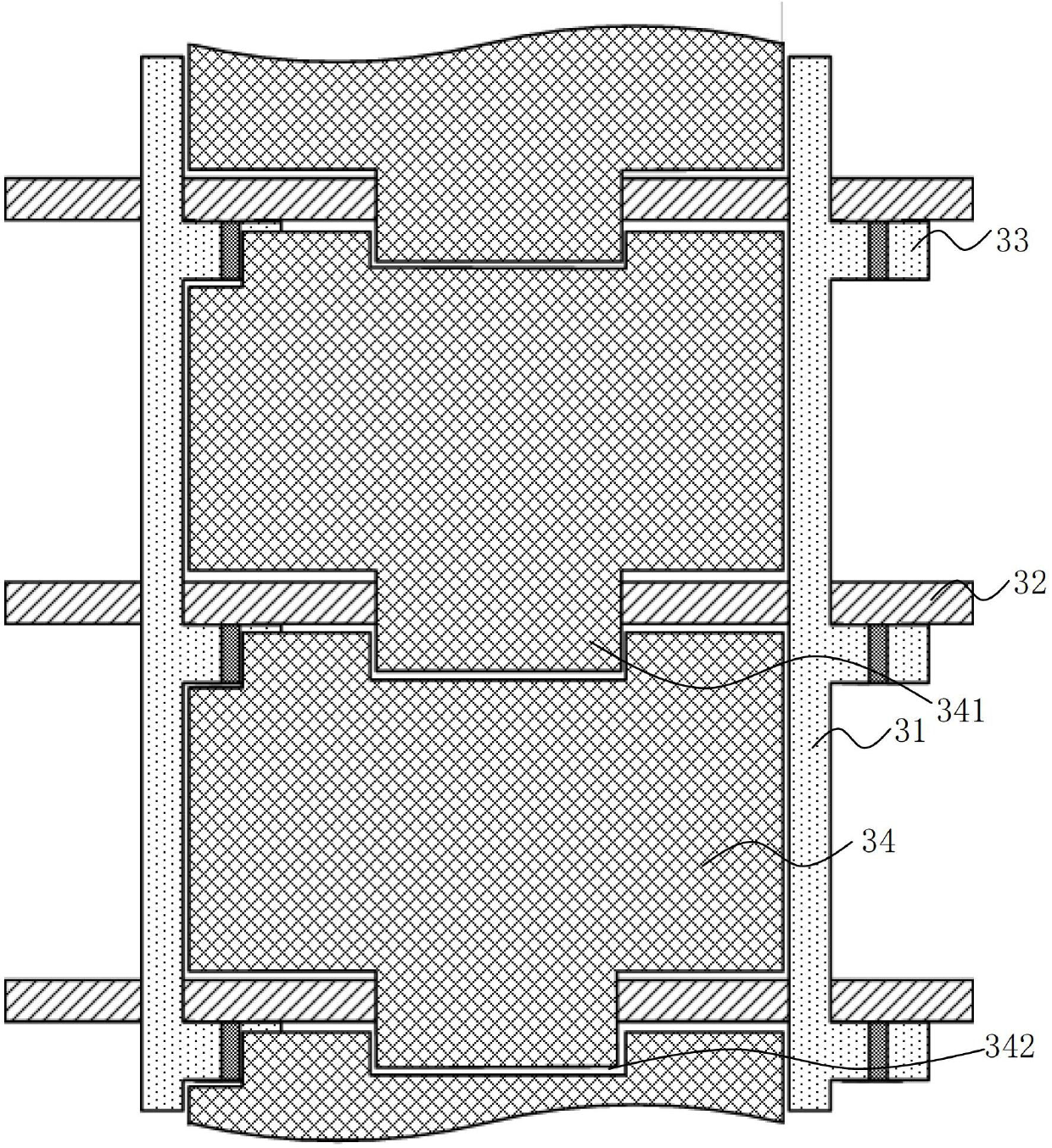
[0027] Please refer to image 3 , image 3 It is a structural schematic diagram of a preferred embodiment of the pixel structure of the present invention. The pixel structure includes a data line 31, a scan line 32, a thin film field effect transistor 33 and a pixel electrode 34. The data line 31 is used to transmit a grayscale signal; the scan line 32 is ...


PUM


Abstract

The invention relates to a pixel structure and a corresponding liquid crystal display device. The pixel structure comprises a data wire, a scanning wire and a pixel electrode; the pixel electrode comprises a crossing part for crossing the scanning wire which is adjacent to the pixel electrode. The pixel structure and the corresponding liquid crystal display device provided by the invention have the advantages of high aperture opening ratio and good manufacturing stability. The technical problem of low aperture opening ratio or poor manufacturing stability of the conventional pixel structure and corresponding liquid crystal display device can be solved.

Description

technical field [0001] The invention relates to the field of liquid crystal display, in particular to a pixel structure with high aperture ratio and good fabrication stability and a corresponding liquid crystal display device. Background technique [0002] The panel size of the current liquid crystal display panel is getting bigger and bigger, and at the same time, users have higher and higher requirements on the wide viewing angle and low energy consumption of the liquid crystal display panel, which promotes the diversified development of the pixel structure design of the liquid crystal display panel. [0003] In each pixel structure of the liquid crystal display panel, a storage capacitor is provided, and the storage capacitor is used to maintain a voltage for driving liquid crystal molecules to rotate. The capacitance value of the storage capacitor should be designed according to the size of the pixel. If the storage capacitor is too small, the above-mentioned driving vol...

Claims


Application Information

Patent Timeline
Patent Type & Authority Applications(China)
IPC IPC(8): G02F1/1343G02F1/1362H01L27/02
CPCG02F1/136213G02F1/134309G02F1/1343G02F2201/40
Inventor 柴立
Owner TCL CHINA STAR OPTOELECTRONICS TECH CO LTD
Learn More