
Amorphous silicon solar cell based on bifacial metal cladding waveguide structure and manufacturing process thereof

A solar cell and waveguide structure technology, applied in the field of solar energy, can solve problems such as narrow absorption range, low photoelectric conversion efficiency, and weak light trapping effect, and achieve low light energy loss, increased light utilization rate, and wide absorption spectrum Effect

Inactive Publication Date: 2014-12-24
UNIV OF SHANGHAI FOR SCI & TECH
View PDF5 Cites 0 Cited by
  • Summary
  • Abstract
  • Description
  • Claims
  • Application Information

AI Technical Summary

Problems solved by technology

However, the existing thin-film amorphous silicon solar cells still have problems such as narrow range of incident angle and absorption range of the spectrum, poor light trapping effect, and low photoelectric conversion efficiency.

Method used


Image

  • Amorphous silicon solar cell based on bifacial metal cladding waveguide structure and manufacturing process thereof
  • Amorphous silicon solar cell based on bifacial metal cladding waveguide structure and manufacturing process thereof

Examples


Embodiment Construction

[0037] In order to make the technical means, creative features, goals and effects achieved by the present invention easy to understand, the present invention will be further described below in conjunction with specific diagrams.

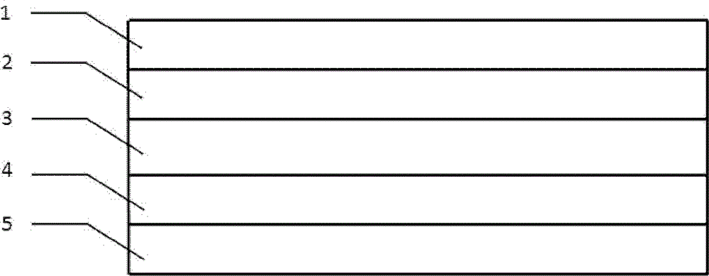
[0038] refer to figure 1 , an amorphous silicon solar cell based on a double-sided metal-clad waveguide structure, comprising a solar cell layer, the solar cell layer comprising a substrate layer, an amorphous silicon layer 4 disposed on the substrate layer, and an amorphous silicon layer 4 disposed on the substrate layer The conductive thin film layer 3, the glass layer 2 arranged on the conductive thin film layer 3, the glass layer 2, the conductive thin film layer 3 and the amorphous silicon layer 4 form a waveguide layer. A metal total reflection layer 5 is used as the substrate layer. It also includes a metal coupling layer 1 , and the metal coupling layer 1 is arranged on the glass layer 2 . The metal coupling layer 1, the waveguide layer and...


PUM


Abstract

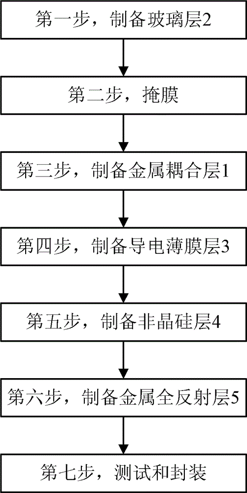
The invention relates to the technical field of solar energy, particularly a solar cell. The amorphous silicon solar cell based on a bifacial metal cladding waveguide structure comprises a solar cell layer, wherein the solar cell layer comprises a substrate layer, an amorphous silicon layer, a conducting film layer and a glass layer, wherein the glass layer, the conducting film layer and the amorphous silicon layer form a waveguide layer; the substrate layer adopts a metal total reflection layer; a metal coupling layer is arranged on the glass layer; and the metal coupling layer, the waveguide layer and the metal total reflection layer form a waveguide structure. The manufacturing method comprises the following steps: 1) preparing the glass layer; 2) preparing the mask; 3) preparing the metal coupling layer; 4) preparing the conducting film layer; 5) preparing the amorphous silicon layer; and 6) preparing the metal total reflection layer. Due to the technical scheme above, the invention has the advantages of wide absorption spectrum, wide spectrum incident angle, high efficiency, strong light trapping effect and the like.

Description

technical field [0001] The invention relates to the technical field of solar energy, in particular to a solar cell. Background technique [0002] At present, the mainstream of solar cells is monocrystalline silicon and polycrystalline silicon, accounting for more than 70% of the world's total annual output of solar cells. However, the cost of this type of solar cell is high, and the semiconductor materials used for production are limited, which is limited by large-scale production. [0003] Therefore, in the whole process from materials to making solar cells, there is an urgent demand for thin-film solar cells that can be continuously manufactured, energy-saving, large-area, light-weight, and can be produced on a large scale. Crystalline silicon (a-Si:H). In 1976, D.E.Conlson and C.R.Wronski of RCA Laboratory in the United States used the photovoltaic (PV) effect to make the world's first a-Si solar cell on the basis of Spear's formation and control of p-n junction work, w...

Claims


Application Information

Patent Timeline
Patent Type & Authority Patents(China)
IPC IPC(8): H01L31/054H01L31/075H01L31/20
CPCY02E10/50Y02E10/52Y02E10/548Y02P70/50
Inventor 陈麟朱亦鸣罗士达陈宏彦
Owner UNIV OF SHANGHAI FOR SCI & TECH
Learn More