Array substrate and liquid crystal display panel
An array substrate and insulating substrate technology, which is applied in the field of liquid crystal display panels, can solve the problems such as the lengthening of the dominant line 78 and the poor disconnection, and achieve the effects of suppressing the reduction of the yield, reducing the size, and suppressing the signal delay.
- Summary
- Abstract
- Description
- Claims
- Application Information
AI Technical Summary
Problems solved by technology
Method used
Image
Examples
Embodiment approach 1
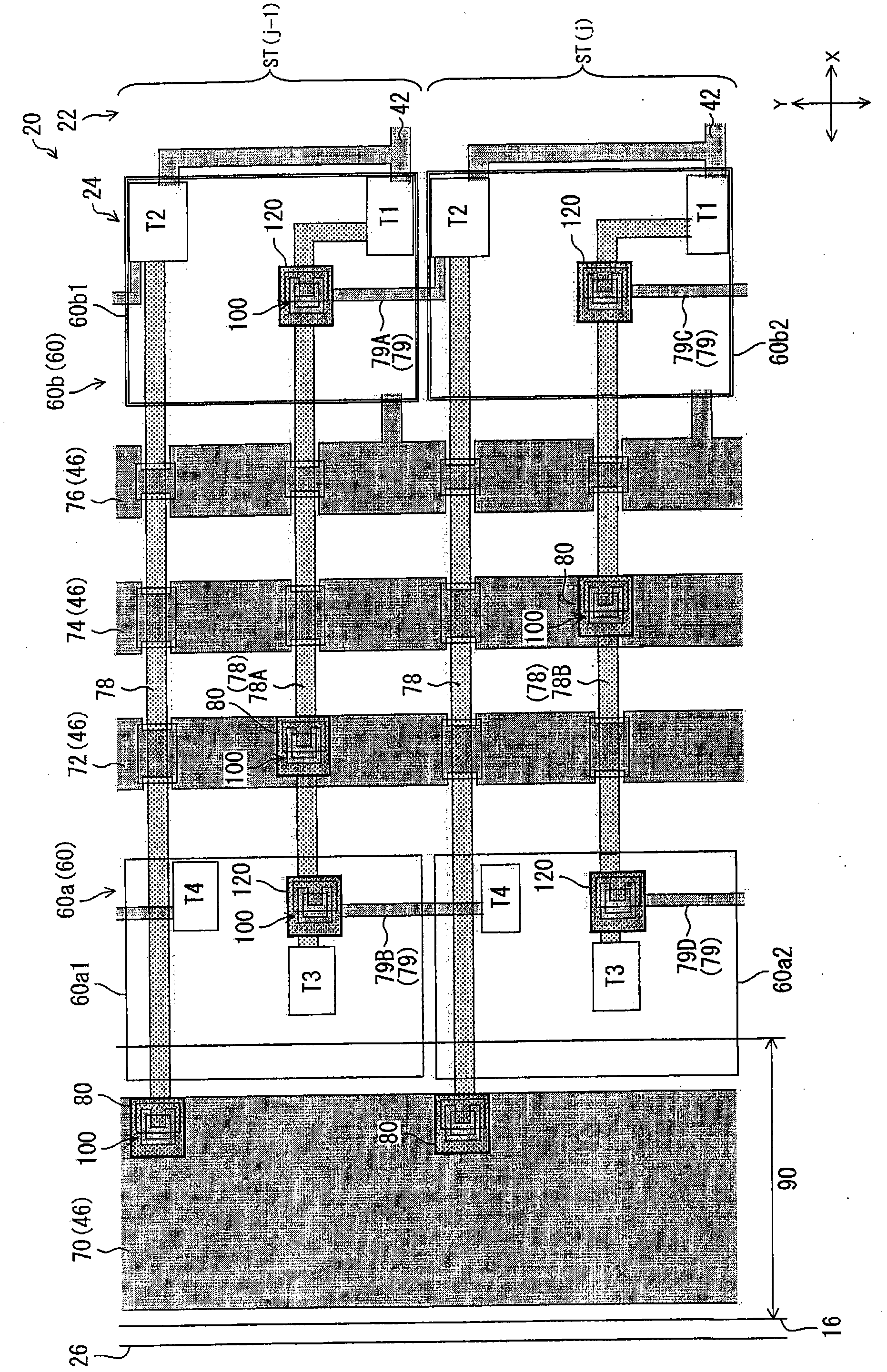
[0078] As shown below, according to Figure 1 ~ Figure 5 An embodiment of the present invention is explained.
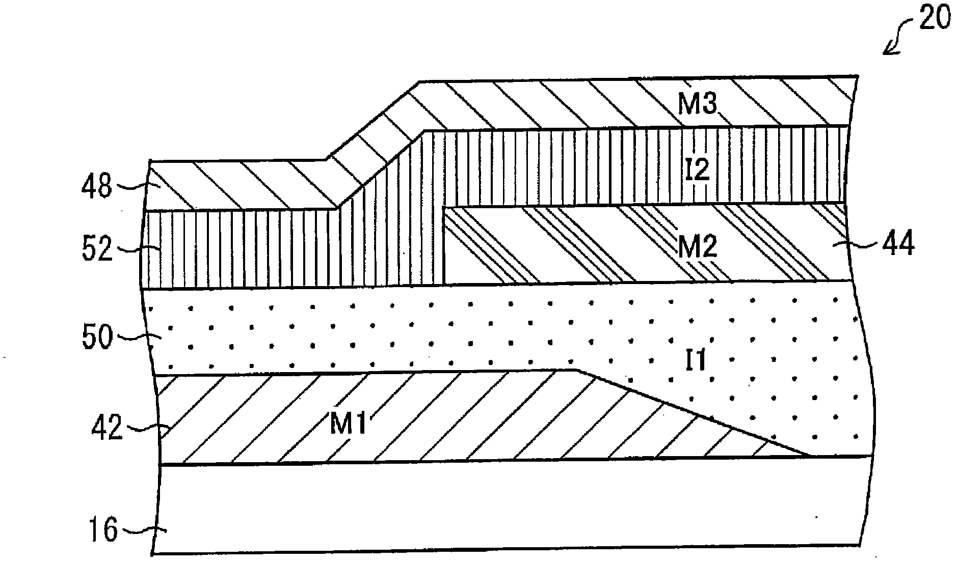
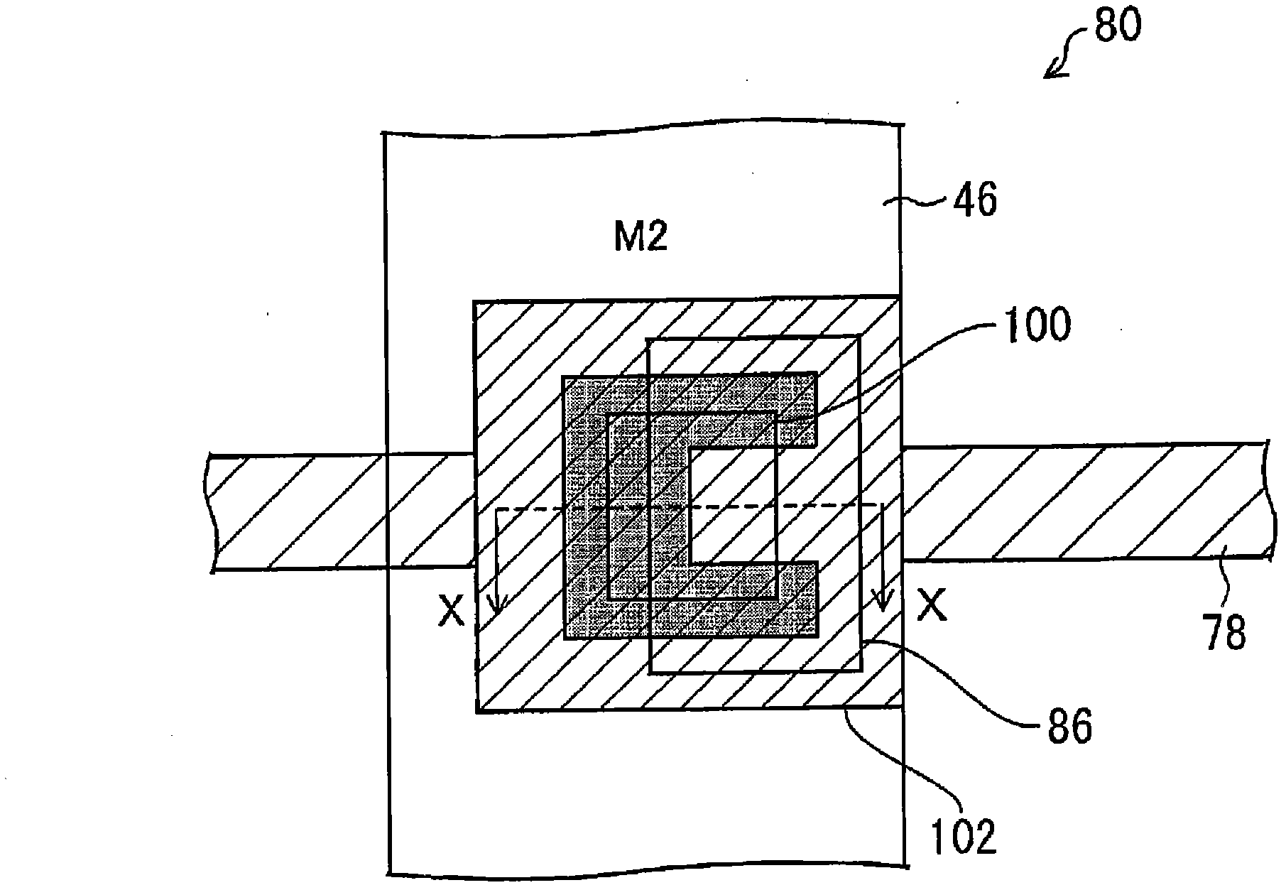
[0079] The TFT array substrate 20 of this embodiment has the basis Picture 12 The TFT array substrate 20 described has substantially the same general configuration.
[0080] figure 1 It is a plan view showing a schematic configuration of the main part of the TFT array substrate 20 of this embodiment.
[0081] Such as figure 1 As shown, in the peripheral area 24 of the TFT array substrate 20 as the array substrate, a gate drive circuit 60 (60a, 60b) and a gate drive circuit wiring 46 connected to an FPC (not shown) are provided. In addition, in the above-mentioned gate drive circuit 60 as a drive circuit, a TFT element as a drive element is formed.
[0082] In the TFT array substrate 20 of this embodiment, the gate drive circuit 60 is divided into two drive circuits in the X direction of the TFT array substrate 20. Specifically, in the X direction described above, the firs...
Embodiment approach 2
[0171] according to Image 6 Other embodiments of the TFT array substrate 20 of the present invention will be described.
[0172] In addition, for convenience of description, members having the same functions as those in the drawings described in the above-mentioned Embodiment 1 are given the same reference numerals, and their description is omitted.
[0173] The TFT array substrate 20 of this embodiment is different from the TFT array substrate 20 of the first embodiment in the form of the wiring 46 for the gate drive circuit. That is, two clock wires have been added. And, accompanying this, the extension method of the branch wiring 79 is different. This is explained below.
[0174] Such as Image 6 As shown, in the peripheral area 24 of the TFT array substrate 20, a gate drive circuit 60 and a gate drive circuit wiring 46 connected to an FPC (not shown) are provided.
[0175] As the gate drive circuit wiring 46, along the Y direction of the TFT array substrate 20, there are provid...
Embodiment approach 3
[0206] As shown below, according to Figure 8 ~ Figure 10 Other embodiments of the TFT array substrate 20 of the present invention will be described.
[0207] In addition, for convenience of description, members having the same functions as those in the drawings described in the above-mentioned respective embodiments are given the same reference numerals, and the description thereof is omitted.
[0208] The TFT array substrate 20 of this embodiment is different from the TFT array substrate 20 of the first embodiment in the form of the connection portion 80 (switching portion 120).
[0209] Figure 8 (A) is a plan view showing an example of the schematic configuration of the connecting portion 80 of this embodiment, Figure 8 (B) is Figure 8 The Y-Y line cross-sectional view of (a).
[0210] Such as Figure 8 As shown, the connecting portion 80 connects the branch wiring 78 and each gate drive circuit wiring 46.
[0211] The branch wiring 78 is formed of the gate wiring 42 layer of the ...
PUM
 Abstract
Description
Claims
Application Information
 - R&D
- Intellectual Property
- Life Sciences
- Materials
- Tech Scout
- Unparalleled Data Quality
- Higher Quality Content
- 60% Fewer Hallucinations
Browse by: Latest US Patents, China's latest patents, Technical Efficacy Thesaurus, Application Domain, Technology Topic, Popular Technical Reports.
© 2025 PatSnap. All rights reserved.Legal|Privacy policy|Modern Slavery Act Transparency Statement|Sitemap|About US| Contact US: help@patsnap.com


