Film removal method, photoelectric conversion device manufacturing method, photoelectric conversion device, and film removal device
A photoelectric conversion device and beam technology, applied in energy conversion devices, photovoltaic power generation, manufacturing tools, etc., can solve problems such as residual film and yield reduction, reduce space, restrain yield reduction, and restrain poor separation. Effect
- Summary
- Abstract
- Description
- Claims
- Application Information
AI Technical Summary
Problems solved by technology
Method used
Image
Examples
Embodiment approach 1
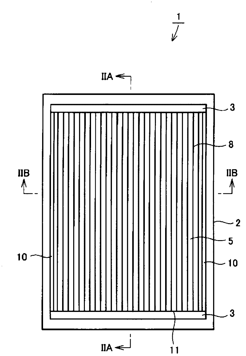
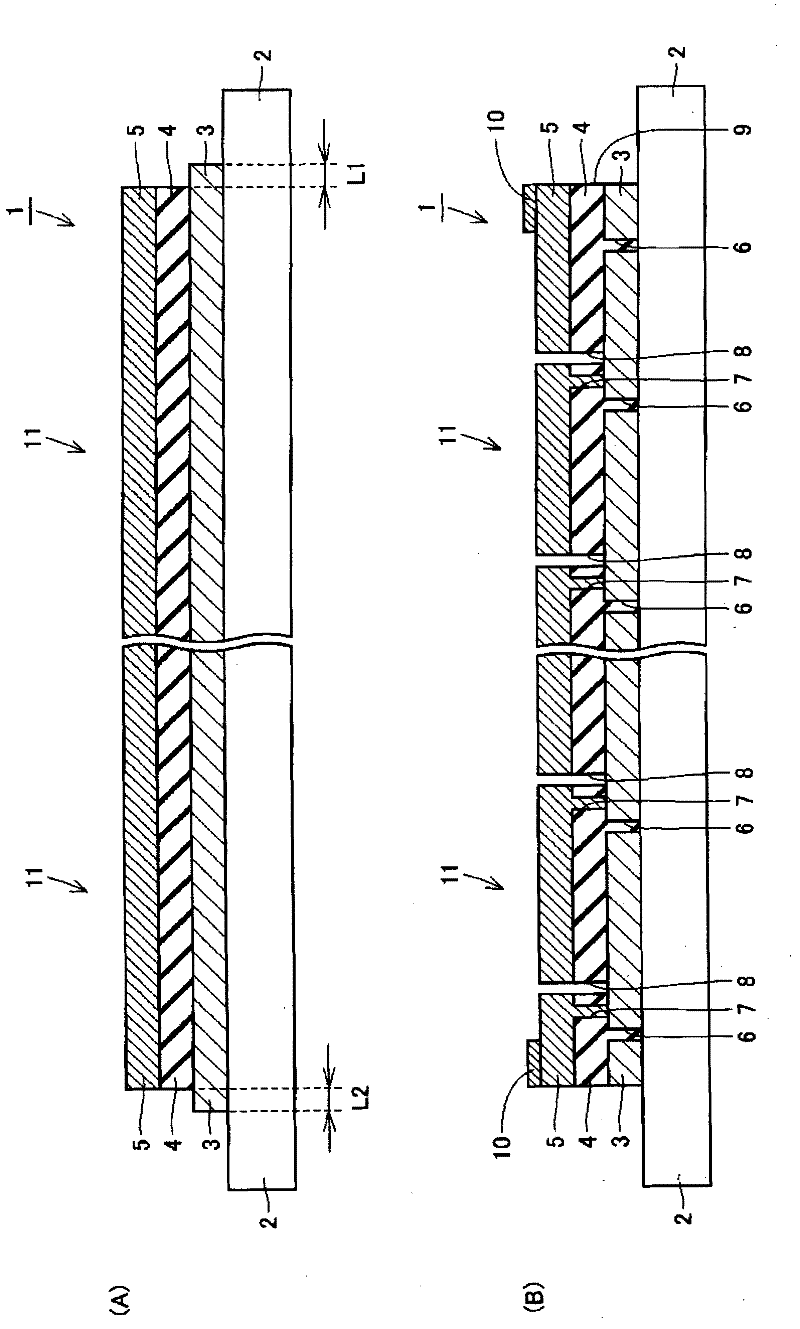
[0064] figure 1 It is a plan view schematically showing the structure of the photoelectric conversion device in Embodiment 1 of the present invention. and, figure 2 (A) and (B) are respectively along figure 1 A schematic cross-sectional view along the line IIA-IIA and along the line IIB-IIB. refer to figure 1 as well as figure 2 A thin-film solar cell 1 as a photoelectric conversion device of this embodiment includes a transparent insulating substrate 2 , a transparent electrode layer 3 , a semiconductor photoelectric conversion layer 4 , a back electrode layer 5 , and an electrode 10 .
[0065] The transparent insulating substrate 2 is a light-transmitting substrate. A transparent electrode layer 3 , a semiconductor photoelectric conversion layer 4 , and a back electrode layer 5 are sequentially stacked on a transparent insulating substrate 2 .
[0066] The transparent electrode layer 3 is a conductive film, and is divided into a plurality of regions by the first sepa...
Embodiment approach 2
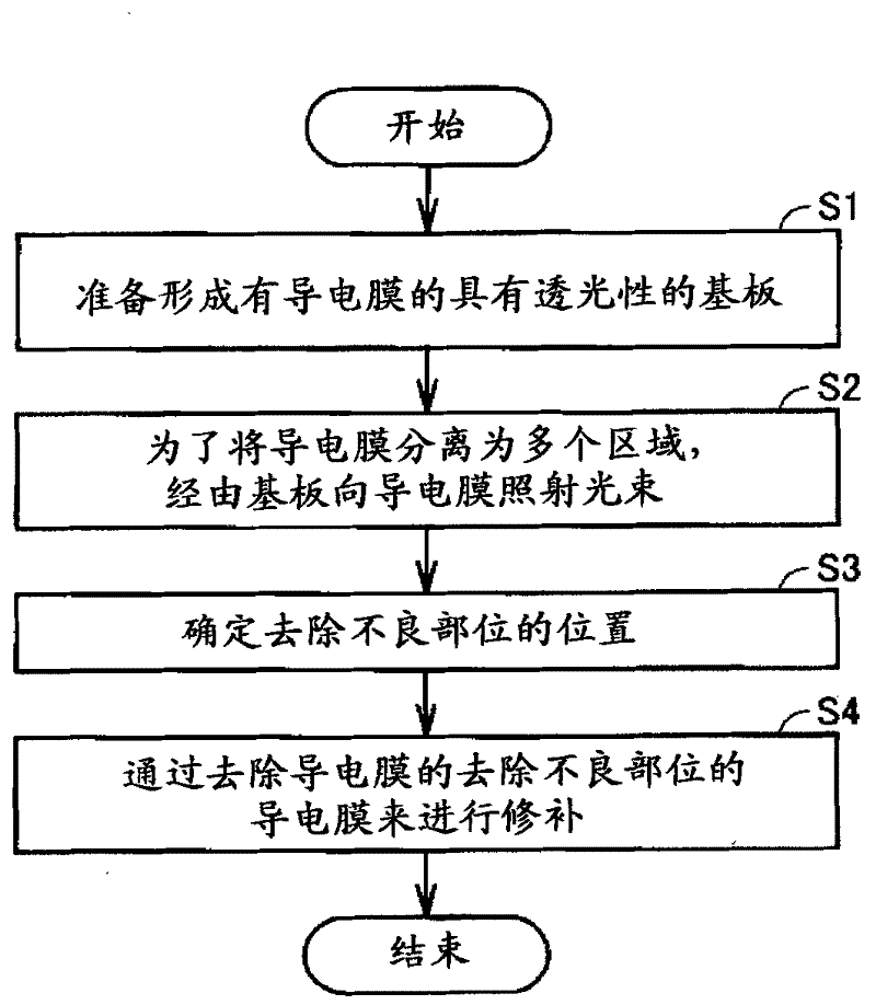
[0102] In this embodiment, in order to perform steps S3 and S4 ( image 3 ) and the film removal device that can be used and how to use it will be described
[0103] Figure 20 It is a perspective view schematically showing the structure of the film removal apparatus in Embodiment 2 of this invention. and Figure 21 is expressed by Figure 20 The block diagram of the composition of each function realized by the film removal device.
[0104] refer to Figure 20 as well as Figure 21 , The film removal device 60 of the present embodiment has: a backup roll 61 (fixed part 610), a probe 62 (resistance measuring part 620), a CCD camera 63 (image recognition part 630), a laser emitting part 64 (processing part 640), an X-Y Manipulator 65 (movement control unit).
[0105] The fixing part 610 has a function of fixing the transparent insulating substrate 2 .
[0106] The resistance measuring unit 620 has a function of measuring the resistance of a specific portion of the transp...
Embodiment approach 3
[0132] In this embodiment, for the above-mentioned Embodiment 1 image 3 Another way of step S4 will be described.
[0133] figure 1 and figure 2 The shown thin-film solar cell 1 as a photoelectric conversion device of this embodiment includes a transparent insulating substrate 2 , a transparent electrode layer 3 , a semiconductor photoelectric conversion layer 4 , a back electrode layer 5 , and an electrode 10 .
[0134] The transparent insulating substrate 2 is a light-transmitting substrate. A transparent electrode layer 3 , a semiconductor photoelectric conversion layer 4 , and a back electrode layer 5 are sequentially stacked on the transparent insulating substrate 2 .
[0135] The transparent electrode layer 3 is a conductive film, and is divided into a plurality of regions by the first separation groove 6 . The first separation groove 6 is filled with the semiconductor photoelectric conversion layer 4 .
[0136] The back electrode layer 5 is a conductive film. Th...
PUM
| Property | Measurement | Unit |
|---|---|---|
| thickness | aaaaa | aaaaa |
| thickness | aaaaa | aaaaa |
Abstract
Description
Claims
Application Information
 - R&D
- Intellectual Property
- Life Sciences
- Materials
- Tech Scout
- Unparalleled Data Quality
- Higher Quality Content
- 60% Fewer Hallucinations
Browse by: Latest US Patents, China's latest patents, Technical Efficacy Thesaurus, Application Domain, Technology Topic, Popular Technical Reports.
© 2025 PatSnap. All rights reserved.Legal|Privacy policy|Modern Slavery Act Transparency Statement|Sitemap|About US| Contact US: help@patsnap.com


