Processing apparatus, transferring apparatus and transferring method

Inactive Publication Date: 2005-02-08
TOKYO ELECTRON LTD
View PDF16 Cites 108 Cited by
  • Summary
  • Abstract
  • Description
  • Claims
  • Application Information

AI Technical Summary

Benefits of technology

The present invention is made for solving the forgoing existing problems. In other words, the present invention is to provide a processing apparatus that can fabricate

Problems solved by technology

However, when the number of thin films is increased, the forgoing six-chamber type processing apparatus 300 that has six processing units cannot deposit all the desired thin films.
In other words, the fabrication efficiency deteriorates.
In addition, since thinner films are required, when a wafer W is taken out from a process atmosphere, a thin film depo

Method used


Image

  • Processing apparatus, transferring apparatus and transferring method
  • Processing apparatus, transferring apparatus and transferring method
  • Processing apparatus, transferring apparatus and transferring method

Examples


first embodiment

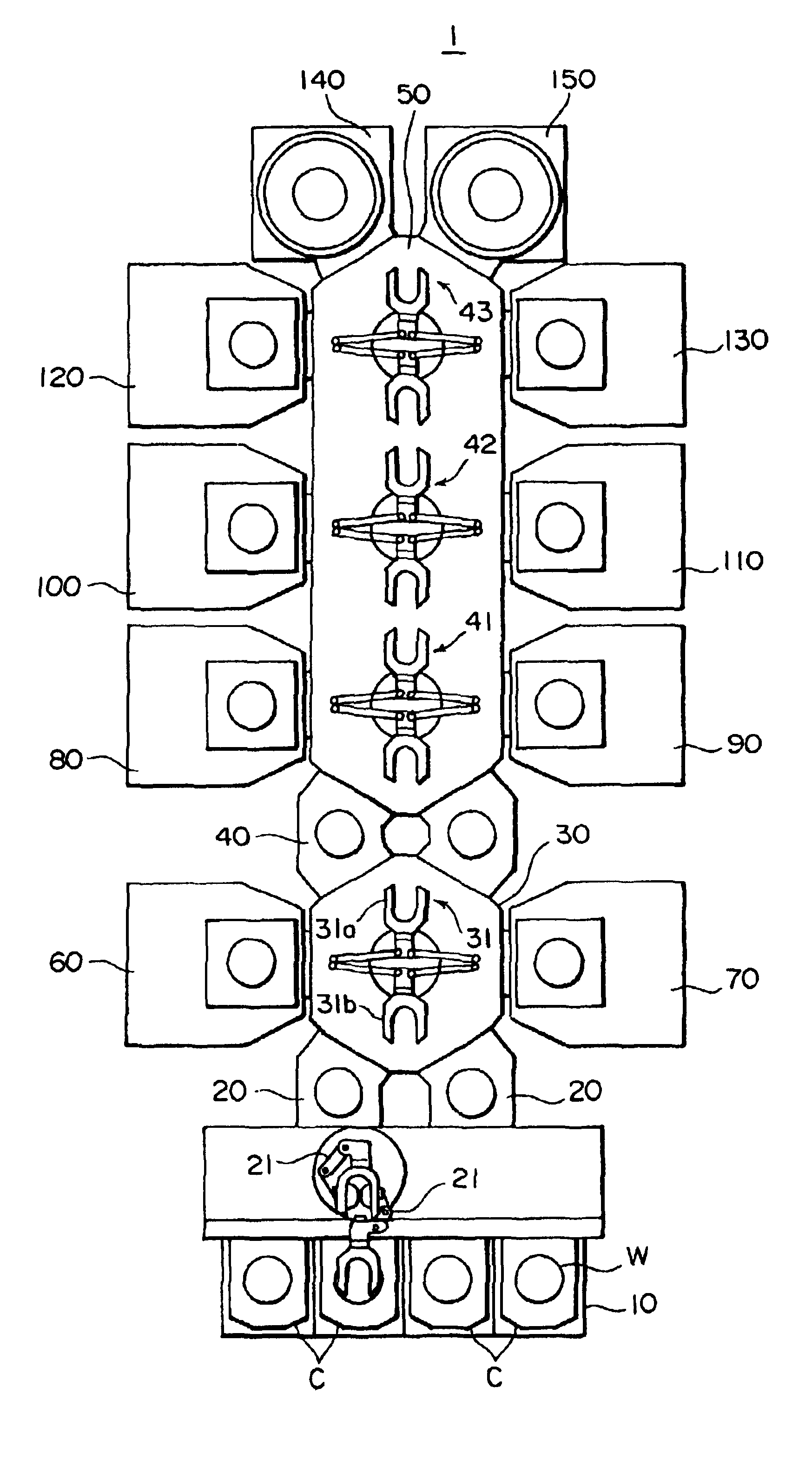
Next, with reference to the accompanying drawings, a first embodiment of the present invention will be explained. FIG. 1 is a plan view showing a processing apparatus 1 according to the first embodiment of the present invention. As shown in FIG. 1, in the processing apparatus 1 according to the first embodiment of the present invention, a substrate container holding table 10, a first transferring chamber 30, and a second transferring chamber 50 are disposed. The substrate container holding table 10 holds a carrier cassette C as a container that can contain a plurality of wafers W (for example, 25 wafers W). The first transferring chamber 30 is disposed on the far side of the substrate container holding table 10. The second transferring chamber 50 is disposed on the far side of the first transferring chamber 30.

A first processing unit group 60, 70 is disposed around the first transferring chamber 30. A second processing unit group 80, 90, 100, 110, 120, 130, 140, and 150 is disposed ...

second embodiment

Next, a second embodiment of the present invention will be explained. FIG. 16 is a plan view showing a processing apparatus 2 according to the second embodiment of the present invention. As shown in FIG. 16, the processing apparatus 2 according to the second embodiment of the present invention has a substrate container holding table 10, a first transferring chamber 30, and a second transferring chamber 50. The substrate container holding table 10 holds a carrier cassette C that contains wafers W. The first transferring chamber 30 is disposed on the far side of the holding table 10. The second transferring chamber 50 is disposed on the far side of the first transferring chamber 30.

A first processing unit group is disposed around the first transferring chamber 30. The first processing unit group is composed of two pre-cleaning units 160 and 170 and two CVD units 180 and 190. The pre-cleaning units 160 and 170 are disposed on the left and right of the first transferring chamber 30, res...

third embodiment

FIG. 21 is a plan view showing an outlined structure of a processing apparatus 3 according to a third embodiment of the present invention. According to the third embodiment, reactive ion etching units 61 and 71 are used instead of supercritical cleaning units used as the pre-cleaning units 60 and 70 of the processing apparatus 1 according to the first embodiment of the present invention. The reactive ion etching units 61 and 71 clean a wafer with a process gas. The reactive ion etching units 61 and 71 are disposed around a transferring chamber 30A together with CVD units 80, 90, 140, and 150 and ALD units 100, 110, 120, and 130 that are used in the next process.

Since the reactive ion etching units 61 and 71 are used in a reduced pressure environment, such units can be laid out. In the processing apparatus according to the third embodiment of the present invention, since many processing units are disposed around the transferring chamber 30A, the processing apparatus having a higher a...


PUM

PropertyMeasurementUnit
Pressureaaaaaaaaaa
Shapeaaaaaaaaaa

Abstract

Processing apparatus is disclosed, that comprises substrate container holding table that can hold substrate container that contains plurality of target substrates, first transferring chamber, disposed adjacent to the substrate container holding table, that maintains the interior at first pressure, first processing unit group, disposed around the first transferring chamber, that processes target substrate at the first pressure, first transferring mechanism, disposed in the first transferring chamber, that transfers target substrate, second transferring chamber, disposed adjacent to the first transferring chamber, that maintains the interior at second pressure, second processing unit group, disposed around the second transferring chamber, that processes target substrate at the second pressure, and second transferring mechanism, disposed in the second transferring chamber, wherein the first transferring mechanism and/or the second transferring mechanism has at least two transferring arms.

Description

BACKGROUND OF THE INVENTION1. Field of the InventionThe present invention relates to a processing apparatus, which processes a target substrate such as a silicon wafer used as a material of a semiconductor device, and a transferring apparatus and a transferring method used for the processing apparatus, in particular, to the processing apparatus that deposits various types of films on the front surface of a target substrate and the transferring apparatus and the transferring method used for the processing apparatus that deposits various types of films on the front surface of a target substrate.2. Description of the Related ArtIn a fabricating method for a semiconductor device that has been widely and conventionally used, various types of thin films such as an oxide film, a nitride film, and a nitrogen oxide film are deposited in a predetermined sectional shape on the front surface of a silicon wafer (that is hereinafter simply referred to as “wafer”). Such various types of thin films...

Claims


Application Information

Patent Timeline
IPC IPC(8): C23C16/54H01L21/00H01L21/677H01L21/67
CPCC23C16/54H01L21/67161H01L21/67167H01L21/67184H01L21/67742H01L21/67745H01L21/67173Y10S414/139
Inventor MATSUSHITA, MINORUKODASHIMA, YASUSHIKUMAI, TOSHIKAZU
Owner TOKYO ELECTRON LTD
Why Eureka
Try Eureka