Semiconductor packaging structure and its module

A packaging structure, semiconductor technology, applied in the direction of semiconductor devices, semiconductor/solid-state device components, electric solid-state devices, etc., can solve the problems of chip cracking under force, limited chip support, reduced chip function and reliability, etc., to avoid coating The effect of uneven glue, preventing chip cracking under force, and improving the quality of chip packaging

Active Publication Date: 2018-02-23
CHINA WAFER LEVEL CSP
View PDF5 Cites 0 Cited by
  • Summary
  • Abstract
  • Description
  • Claims
  • Application Information

AI Technical Summary

Problems solved by technology

However, for larger chips, the support of the single-layer spacer for the chip is limited, and it is easy to cause problems such as cracking of the chip during the subsequent manufacturing process, which will inevitably reduce the function and reliability of the chip.

Method used


Image

  • Semiconductor packaging structure and its module
  • Semiconductor packaging structure and its module
  • Semiconductor packaging structure and its module

Examples


Embodiment Construction

[0022] The present invention will be described in detail below in conjunction with specific embodiments shown in the accompanying drawings. However, these embodiments do not limit the present invention, and any structural, method, or functional changes made by those skilled in the art according to these embodiments are included in the protection scope of the present invention.

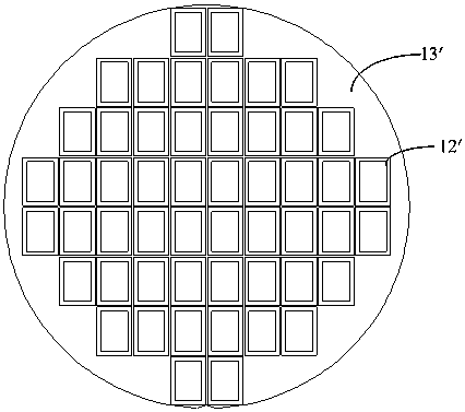
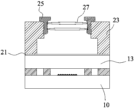
[0023] Such as image 3 As shown, the semiconductor module according to an embodiment of the present invention includes a semiconductor package structure, a lens assembly, and a filter layer 21 arranged between the semiconductor package structure and the lens assembly, wherein the lens assembly includes A lens container 23 , a lens bracket 25 disposed in the lens container 23 , and at least one lens 27 fixedly arranged by the lens bracket 25 .

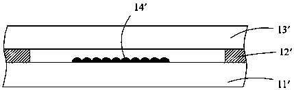
[0024] Such as Figure 4 As shown, in a preferred embodiment of the present invention, the packaging structure includes a chip 10 and a substrate 13, because...


PUM


Abstract

The invention discloses a packaging structure, comprising: a chip with an optical electronic device formed on one side, and a substrate covering the chip; a main spacer is provided between the chip and the substrate, and the feature is that the chip and the substrate At least one layer of spacers between the optical electronic device and the main spacer is also provided between the substrates. Compared with the prior art, the present invention prevents the cracking of the chip caused by the force of the chip due to the excessive size of the chip by setting the secondary spacer between the optical electronic device and the main spacer, and avoids the excessive widening of the spacer. The problem of uneven glue coating is caused, thereby improving the quality of chip packaging.

Description

technical field [0001] The invention relates to the technology in the field of semiconductor manufacturing, in particular to a semiconductor packaging structure and a module thereof. Background technique [0002] Wafer Level Chip Size Packaging (WLCSP) is a technology that packages and tests the entire wafer and then cuts it to obtain a single finished chip. Among them, this technology mainly protects the optical and electronic devices of the wafer chip by covering the optical and electronic devices with a piece of high-transparency glass with multiple spacers. Such as figure 1 , figure 2 As shown, in the prior art, wafer chips are packaged using a high-transparency glass 13' with a plurality of spacers 12', wherein the spacers are formed in the following way: on a high-transparency glass 13 ', spin-coat a layer of photoresist, and then form a ring of spacers 12' by exposure and development, and then pass the entire piece of high light-transmitting glass with spacers and...

Claims


Application Information

Patent Timeline
Patent Type & Authority Patents(China)
IPC IPC(8): H01L23/00H01L23/31
Inventor 王文龙喻琼俞国庆沈戌霖王蔚
Owner CHINA WAFER LEVEL CSP
Why Eureka
Try Eureka