Semiconductor packaging piece, stack packaging piece using semiconductor packaging piece and manufacturing method of semiconductor packaging piece

A manufacturing method and packaging technology, which is applied in semiconductor/solid-state device manufacturing, semiconductor/solid-state device components, semiconductor devices, etc., can solve the problems of large stacked packaging structure size and the inability to effectively increase the number of output/input contacts

Inactive Publication Date: 2012-10-24
ADVANCED SEMICON ENG INC
View PDF3 Cites 14 Cited by
  • Summary
  • Abstract
  • Description
  • Claims
  • Application Information

AI Technical Summary

Problems solved by technology

[0003] However, the size of the stacked package structure is too large due to the side-arranged chips, and the stacked package structure that provides I / O functions on one side cannot effectively increase the number of I / O contacts, thus limiting the traditional stacked package structure. application of structure

Method used


Image

  • Semiconductor packaging piece, stack packaging piece using semiconductor packaging piece and manufacturing method of semiconductor packaging piece
  • Semiconductor packaging piece, stack packaging piece using semiconductor packaging piece and manufacturing method of semiconductor packaging piece
  • Semiconductor packaging piece, stack packaging piece using semiconductor packaging piece and manufacturing method of semiconductor packaging piece

Examples


Embodiment Construction

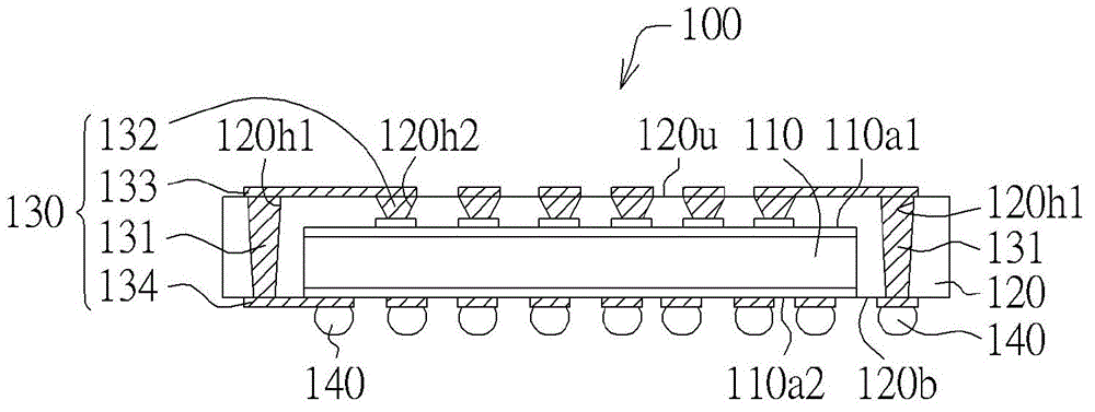
[0054] Please refer to figure 1 , which shows a cross-sectional view of a semiconductor package according to an embodiment of the present invention. The semiconductor package 100 includes a chip component 110 , a package body 120 , a connector 130 and at least one electrical contact 140 .

[0055] The chip component 110 is, for example, a single chip, such as a silicon chip. Here, a single chip refers to a chip cut by the same dicing process, or a chip formed by the same semiconductor process, and it is not a combination of two diced chips. The chip component 110 has a first active surface 110a1 and a second active surface 110a2 opposite to each other, wherein the first active surface 110a1 is covered by the package body 120 . The second active surface 110 a 2 is not covered by the package body 120 , but exposed from the second surface 120 b of the package body 120 .

[0056] The package body 120 covers the chip component 110 and has at least one through hole 120h1 and a fi...


PUM


Abstract

The invention discloses a semiconductor packaging piece, a stack packaging piece using the semiconductor packaging piece and a manufacturing method of the semiconductor packaging piece. The semiconductor packaging piece comprises a chip element, a packaging body and a connecting piece; the chip element is provided with a first active surface and a second active surface which are opposite to each other; the packaging body is used for wrapping the chip element and is provided with a through hole; the connecting piece is electrically connected with the first active surface and the second active surface of the chip element through a through hole and exposes out of the semiconductor packaging piece.

Description

technical field [0001] The present invention relates to a semiconductor package, a stacked package using the same and a manufacturing method thereof, and in particular to a conductive semiconductor package with input / output functions on both sides, and a stacked package using the same components and methods of manufacture. Background technique [0002] The traditional stacked package structure includes a plurality of chips arranged sideways. These chips usually only have a single active surface and face the same direction, so that the stacked package structure becomes a structure with a single side providing I / O functions. [0003] However, the size of the stacked package structure is too large due to the side-arranged chips, and the stacked package structure that provides I / O functions on one side cannot effectively increase the number of I / O contacts, thus limiting the traditional stacked package structure. Application of structure. Contents of the invention [0004] T...

Claims


Application Information

Patent Timeline
Patent Type & Authority Applications(China)
IPC IPC(8): H01L23/488H01L25/00H01L21/48
CPCH01L21/568H01L24/82H01L24/96H01L2224/0401H01L2224/04105H01L2224/06181H01L2224/12105H01L2224/19H01L2224/24H01L2224/2518H01L2224/32145H01L2224/73267H01L2224/9222H01L2224/92244H01L2225/1035H01L2225/1058H01L2225/107H01L2224/18H01L2924/00012
Inventor 颜瀚琦
Owner ADVANCED SEMICON ENG INC
Why Eureka
Try Eureka