Splinter device and method of wafer
A technology of wafers and splits, which is applied in the manufacture of electrical components, semiconductor/solid-state devices, circuits, etc., can solve the problems of low split efficiency, chip crack damage, and unable to adjust the force, and achieve high efficiency and improve the yield.
- Summary
- Abstract
- Description
- Claims
- Application Information
AI Technical Summary
Problems solved by technology
Method used
Image

Examples
Embodiment 1
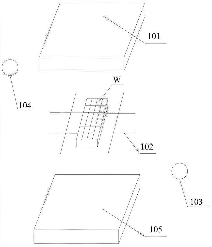
[0027] see figure 1 , Embodiment 1 of the present invention provides a wafer splitting device, the device includes an ultrasonic transducer 101 for generating ultrasonic waves, and a transmission medium for transmitting ultrasonic waves to wafers W after dicing ( figure 1 not shown in ), and a support 102 for supporting the diced wafer W. Wherein, the ultrasonic transducer 101 and the support member 102 are arranged opposite to each other.
[0028] Wherein, the wafer W after dicing may be a wafer for manufacturing light-emitting diodes, laser diodes, superluminescent light-emitting diodes, and the like. It is known that several chips are grown on the wafer; the splitting operation of the wafer is to split the wafer to obtain several individual chips. The wafer W after dicing is the wafer after the dicing operation is completed. Specifically, the wafer can be diced by using ultraviolet laser or stealth dicing technology. Generally, the ultraviolet laser scribing technology ...
Embodiment 2
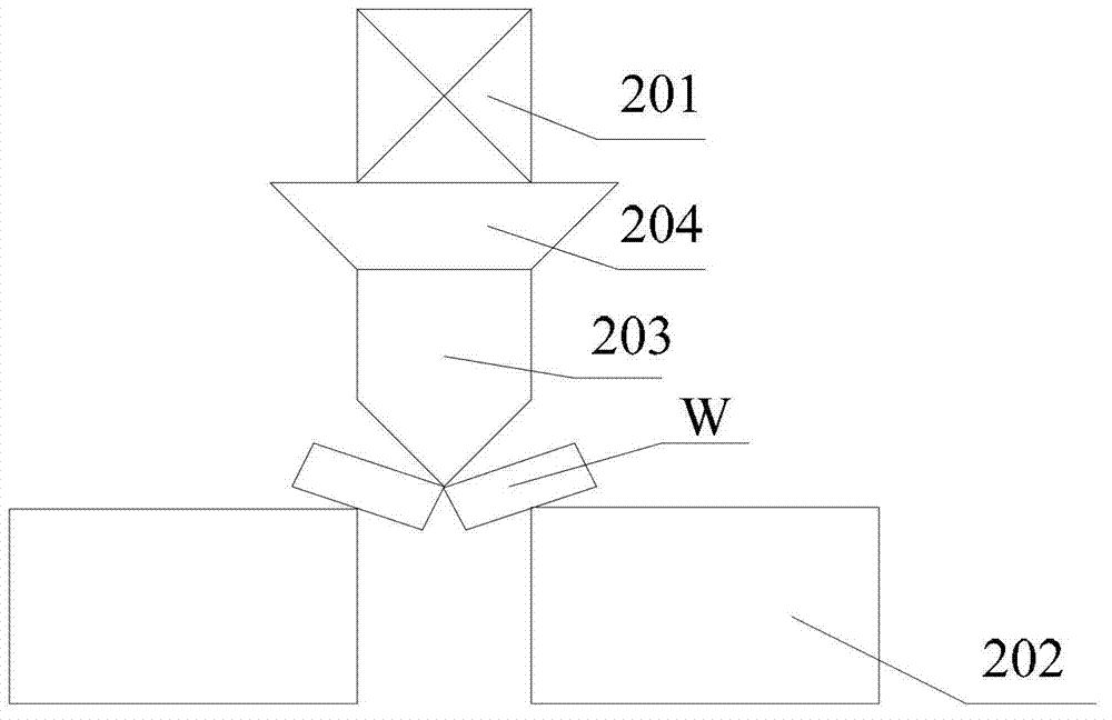
[0039] see figure 2 , Embodiment 2 of the present invention provides a wafer splitting device, the device includes an ultrasonic transducer 201 for generating ultrasonic waves, a transmission medium for transmitting ultrasonic waves to the wafer W after dicing, and a support for A support 202 for the wafer W after dicing. Wherein, the transmission medium is a rivet 203 for splitting the wafer W after dicing; the device also includes a horn 204 for adjusting the amplitude of the ultrasonic waves, and an adjustment assembly for adjusting the position of the rivet 203 ( figure 2not shown). Wherein, the ultrasonic transducer 201 is connected with one end of the horn 204 . The other end of the horn 204 is provided on the splitting knife 203 . The rivet 203 is connected with the adjustment assembly and is arranged directly above the support member 202 .
[0040] Wherein, the ultrasonic transducer 201 and the support member 202 are the same as the ultrasonic transducer 101 and ...
Embodiment 3
[0049] Embodiment 3 of the present invention provides a method for splitting a wafer, the method comprising:
[0050] 301 : Contact the diced wafer with an ultrasonic transmission medium.
[0051] Specifically, as described in Embodiment 1 of the present invention, the transmission medium of the ultrasonic wave is a transparent substance, including air, purified water, alcohol, acetone or glass. If air is used as the transmission medium of ultrasonic waves, then only the diced wafers need to be placed in the air. In practical application, since pure water and other substances transmit ultrasonic waves better than air and are transparent, pure water and other substances should be selected as the ultrasonic transmission medium as much as possible.
[0052] 302: Propagate ultrasonic waves to the diced wafers in the transmission medium, so that the diced wafers are split under the action of ultrasonic waves.
[0053] Wherein, the frequency of the ultrasonic waves can be changed ...
PUM
 Abstract
Description
Claims
Application Information
 - R&D Engineer
- R&D Manager
- IP Professional
- Industry Leading Data Capabilities
- Powerful AI technology
- Patent DNA Extraction
Browse by: Latest US Patents, China's latest patents, Technical Efficacy Thesaurus, Application Domain, Technology Topic.
© 2024 PatSnap. All rights reserved.Legal|Privacy policy|Modern Slavery Act Transparency Statement|Sitemap