

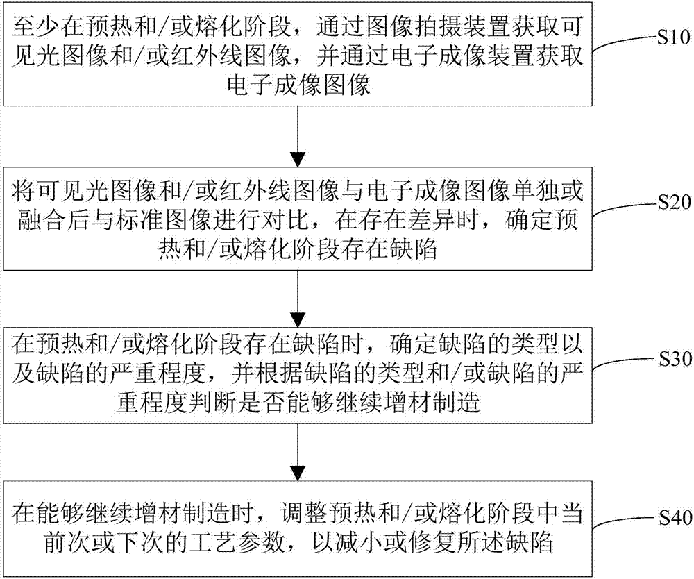
Additive manufacturing defect detection method and additive manufacturing apparatus
A technology of additive manufacturing and defect detection, applied in the field of additive manufacturing, can solve problems such as image information misdetection or missed detection, detection lag, etc., to achieve the effect of increasing yield, reducing defect generation, and avoiding defect detection lag
- Summary
- Abstract
- Description
- Claims
- Application Information
AI Technical Summary
Problems solved by technology
Method used
Image

Examples
example 1
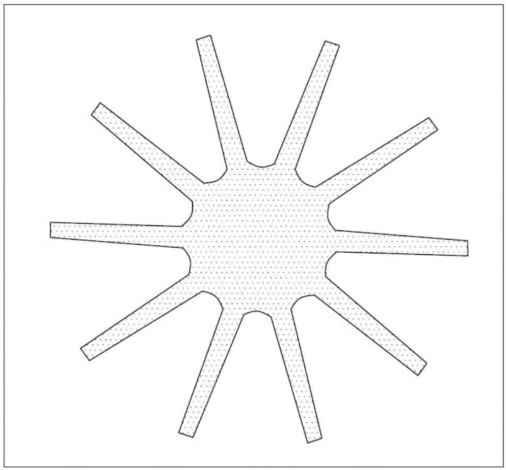
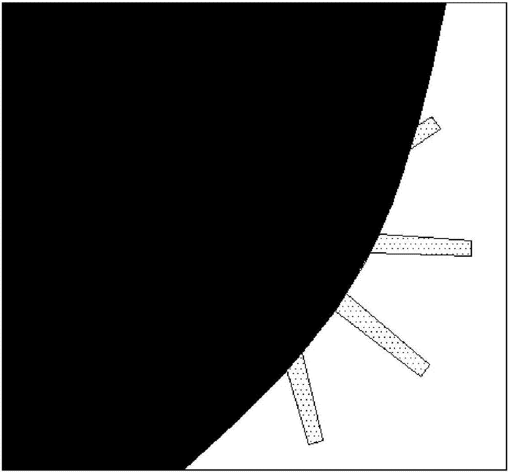
[0064] Example 1: can refer to figure 2 , figure 2 is a schematic diagram of the above standard image, which at this time shows the control image of the current unprocessed powder thin layer or the visible light image before the powder is not scraped. image 3 is the fused imaging image obtained after the warm-up scan of the visible light image and the electronic imaging image fused, from image 3 It can be seen that due to the uneven laying of the powder thin layer, there will be no powder coverage or less powder coverage on the lower right side, and the visible light image can identify two areas, one part with thicker powder layer and one part with thinner powder. However, the printed area may not necessarily be recognized. The electronic imaging device can recognize the printed area. By fusing the visible light image with the electronic imaging image, a clear powder layer distribution and an image of the printed area can be obtained. figure 2 By comparison, the powder ...
example 2
[0065] Example 2: In this example, Figure 4 It is a schematic diagram of the fusion imaging image after the fusion of visible light image and infrared image, which contains topography and heat distribution information; Figure 5 It is a schematic diagram of the fusion imaging image obtained by the fusion of the secondary electron image obtained from the electron imaging image and the backscattered electron image, which contains the morphology and composition distribution information; Image 6 It is a schematic diagram of the fused imaging image after the fusion of visible light image, infrared image and electronic imaging image, which contains various information such as morphology, heat distribution, and composition distribution. can Figure 4 and Figure 5 respectively with figure 2 In contrast, at this time Figure 4 shows the existence of morphological defects B, Figure 5 It also shows that there is a morphological defect B in the powder, so it can be accurately ju...
PUM
| Property | Measurement | Unit |
|---|---|---|
| particle diameter | aaaaa | aaaaa |
Abstract
Description
Claims
Application Information