Stack-based light-emitting diode and manufacturing method thereof

A technology of light-emitting diodes and manufacturing methods, which is applied to electrical components, circuits, semiconductor devices, etc., can solve the problems of complex packaging and wiring, poor color mixing of warm white light-emitting diodes, etc., and achieve simple packaging and wiring, good color mixing, and manufacturing methods. simple effect

Inactive Publication Date: 2012-12-12
合肥彩虹蓝光科技有限公司
View PDF4 Cites 2 Cited by
  • Summary
  • Abstract
  • Description
  • Claims
  • Application Information

AI Technical Summary

Problems solved by technology

[0005] In view of the above-mentioned shortcomings of the prior art, the purpose of the present invention is to provide a stacked light-emitting diode and its manuf

Method used


Image

  • Stack-based light-emitting diode and manufacturing method thereof
  • Stack-based light-emitting diode and manufacturing method thereof
  • Stack-based light-emitting diode and manufacturing method thereof

Examples


Embodiment 1

[0059] Such as Figure 10As shown, this embodiment provides a stacked light emitting diode, the stacked light emitting diode at least includes:

[0060] A supporting structure, which includes a supporting substrate 13 and a lower electrode 15 bonded to the lower surface of the supporting substrate 13;

[0061] The reflective layer 12 is combined on the upper surface of the supporting substrate 13;

[0062] The first color light-emitting layer 11 is combined on the surface of the reflective layer 12;

[0063] A transparent conductive layer 14, bonded to the surface of the first color light-emitting layer 11;

[0064] The second color light-emitting layer 21 is combined on the surface of the transparent conductive layer 14;

[0065] Phosphor powder of a third color, coated on the surface of the light-emitting layer 21 of the second color;

[0066] The upper electrode 24 is combined with the surface of the second color light emitting layer 21 .

[0067] In this embodiment, t...

Embodiment 2

[0072] Such as Figure 1 to Figure 10 As shown, this embodiment provides a method for manufacturing a stacked light emitting diode, which at least includes the following steps:

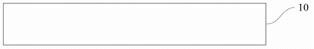
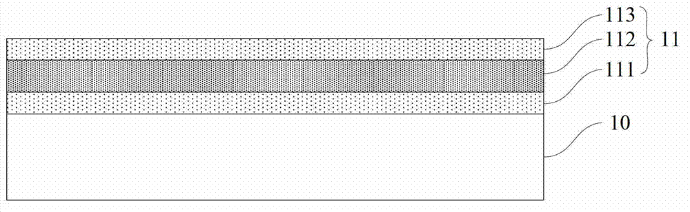
[0073] Such as Figure 1~2 As shown, step 1) is performed first, providing a first substrate 10 , and forming a first color light-emitting layer 11 on the surface of the first substrate 10 .

[0074] In this embodiment, the first substrate 10 is a GaAs substrate, and the first color is red. Specifically, N-AlGaP layer 111, Al x Ga y In (1-x-y) The P layer 112 and the P-AlGaP layer 113 form the first color light emitting layer 11, wherein 0

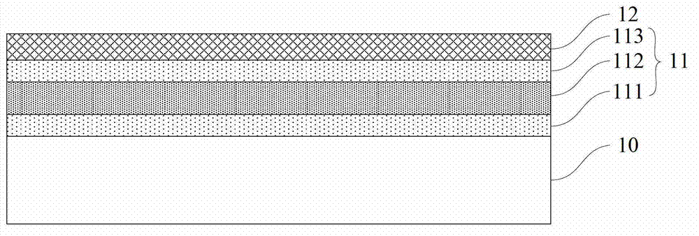
[0075] Such as image 3 As shown, then step 2) is performed to form a reflective layer 12 on the surface of the first color light-emitting layer 11 .

[0076] In this embodiment, th...


PUM


Abstract

The invention provides a stack-based light-emitting diode and a manufacturing method thereof. The stack-based light-emitting diode comprises a support structure, a reflecting layer, a first colour luminescent layer, a transparent conducting layer, a second colour luminescent layer, a third colour phosphor powder and an upper electrode, wherein the support structure is provided with a support substrate and combined with a lower electrode on the lower surface of the support substrate; the a reflecting layer is combined on the upper surface of the support substrate; the first colour luminescent layer is combined on the surface of the reflecting layer; the transparent conducting layer is combined on the surface of the first colour luminescent layer; the second colour luminescent layer is combined on the surface of the transparent conducting layer; the third colour phosphor powder is coated on the surface of the second colour luminescent layer; and the upper electrode is combined on the surface of the second colour luminescent layer. The warm white light-emitting diode provided by the invention has the advantages that the packaging connection is simple, the color mixing property is good, the manufacturing method is simple, the manufacture method has the conventional light-emitting diode manufacturing process, and the manufacturing method is suitable for industrial production.

Description

technical field [0001] The invention belongs to the field of semiconductor lighting, in particular to a stacked light-emitting diode and a manufacturing method thereof. Background technique [0002] As a new type of high-efficiency solid light source, semiconductor lighting has significant advantages such as long life, energy saving, environmental protection, and safety. It will become another leap in the history of human lighting after incandescent lamps and fluorescent lamps. The upgrading of the industry and other industries has huge economic and social benefits. Because of this, semiconductor lighting is generally regarded as one of the most promising emerging industries in the 21st century, and also one of the most important commanding heights in the field of optoelectronics in the next few years. Light-emitting diodes are made of III-IV compounds, such as GaAs (gallium arsenide), GaP (gallium phosphide), GaAsP (gallium arsenide phosphide) and other semiconductors, and...

Claims


Application Information

Patent Timeline
IPC IPC(8): H01L33/50H01L33/62H01L33/00
Inventor 陈吉兴
Owner 合肥彩虹蓝光科技有限公司
Why Eureka
Try Eureka