Supercharge Your Innovation With Domain-Expert AI Agents!

A ligbt device with esd protection

An ESD protection and device technology, which is applied in the field of power semiconductors and can solve problems such as loss, permanent damage to semiconductor devices or integrated circuits, etc.

Inactive Publication Date: 2014-10-29
UNIV OF ELECTRONICS SCI & TECH OF CHINA +1
View PDF2 Cites 0 Cited by
  • Summary
  • Abstract
  • Description
  • Claims
  • Application Information

AI Technical Summary

Problems solved by technology

[0002] Electrostatic discharge is a common phenomenon in the process of manufacturing, packaging, testing, storage, and use of semiconductor devices or integrated circuits, which often causes permanent damage to semiconductor devices or integrated circuits, and thus causes serious losses

Method used


Image

  • A ligbt device with esd protection
  • A ligbt device with esd protection
  • A ligbt device with esd protection

Examples


no. 1 approach

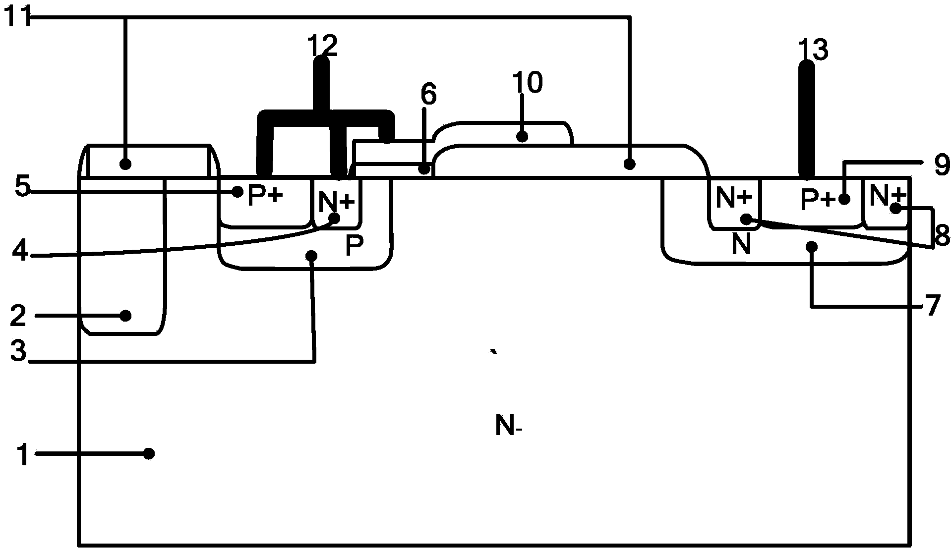
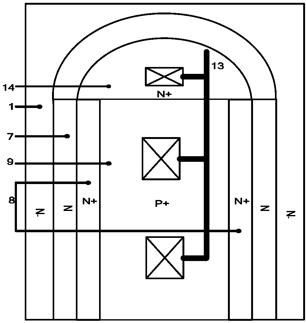
[0018] A LIGBT device with ESD protection, such as figure 1 , 3 As shown, it includes an N-drift region 1, a P-type well region 3 and an N-type well region 7 located on both sides of the top of the N-drift region 1; an N+ doped cathode is arranged in the P-type well region 3 region 4 and a P+ doped P well contact region 5, the N+ doped source region 4 and the P+ doped P well contact region 5 are in contact with each other or are isolated from each other; the N type well region 7 is provided with P+ The doped anode region 9 and the N+ doped N well contact region 8 in contact with the P+ doped anode region 9 are provided with junction terminal N+ doped N in the N-type well region 7 of the entire device junction terminal. Well contact region 14; N-drift region 1 is provided with an isolation region 2 near the P-type well region 3 and away from the N-type well region 7, which is used for mutual isolation between the LIGBT device and other devices; the gate oxide layer of the devi...

no. 2 approach

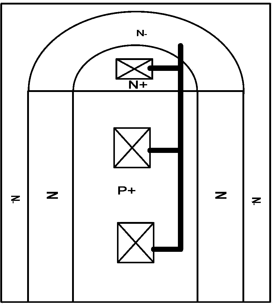
[0021] The second embodiment is a modification based on the first embodiment, the difference mainly lies in the layout of the P+ doped anode region 9 in contact with the N+ doped N well contact region 8 around it. like Figure 5 As shown, on the basis of the first embodiment, the area of ​​the P+ doped anode region 9 is reduced, and the P+ doped anode region 9 and the N+ doped N well contact region 8 are arranged side by side, and the P+ doped anode region 9 is provided with a contact hole and the N+ doped N well contact region 8 is not provided with a contact hole.

[0022] The difference between the present invention and the traditional LIGBT device is that the present invention not only sets the junction terminal N+ doped N well contact region 14 in the N type well region 7 of the anode junction terminal (channel width direction), but also the P+ doped An N+ doped N well contact region 8 is also provided around the anode region 9 (no contact hole is provided in the N+ dope...


PUM


Abstract

The invention relates to a lateral insulator gate bipolar transistor (LIGBT) device with an electronic static discharge (ESD) protection function, which belongs to the technical field of a power semiconductor device. On the premise that a masking template and technical procedures are not increased, an LIGBT device with the ESD protection function is provided by optimizing the device structure and domain. The LIGBT device is different from the traditional insulator gate bipolar transistor (IGBT) device that not only is an end terminal N+ doped N-pit contact area (14) arranged on an anode end terminal (in the width direction of a channel), but also an N+ doped N-pit contact area (8) is arranged on the periphery of a P+ doped anode area (9), the parasitic resistance of an N-type buffering area is reduced through the optimization of the device structure and domain, the starting voltage of a register PNP pipe of the device is increased, and the failure current is remarkably improved by 20 percent compared with the traditional IGBT device unit.

Description

technical field [0001] The invention belongs to the technical field of power semiconductor devices, and relates to an electrostatic discharge (Electro-static Discharge, ESD for short) protection circuit of an integrated circuit chip, especially a LIGBT (Lateral Insulated Gate Bipolar Transistor) with ESD protection function. transistor) device structure. Background technique [0002] Electrostatic discharge is a common phenomenon in the process of manufacturing, packaging, testing, storage, and use of semiconductor devices or integrated circuits, which often causes permanent damage to semiconductor devices or integrated circuits, and thus causes serious losses. In order to solve this problem, a protection circuit is often designed between the internal circuit and the I / O port, and between the positive and negative power rails in chip design. The function of this protection circuit is to prevent the pulse current of electrostatic discharge from flowing into the internal circu...

Claims


Application Information

Patent Timeline
Patent Type & Authority Patents(China)
IPC IPC(8): H01L27/02H01L29/739
Inventor 蒋苓利张波何川吴道训樊航
Owner UNIV OF ELECTRONICS SCI & TECH OF CHINA
Features
  • R&D
  • Intellectual Property
  • Life Sciences
  • Materials
  • Tech Scout
  • Unparalleled Data Quality
  • Higher Quality Content
  • 60% Fewer Hallucinations
Learn More