Electrostatic protection structure and forming method thereof

A technology of electrostatic protection and electrical connection structure, applied in the direction of circuits, electrical components, electrical solid devices, etc., can solve the problems of lack of protection effect, low maintenance voltage, and reduced economic benefits, so as to increase the probability of latch-up effect, Improve the effect of sustaining voltage drop

Pending Publication Date: 2022-03-25
HUA HONG SEMICON WUXI LTD
View PDF0 Cites 0 Cited by
  • Summary
  • Abstract
  • Description
  • Claims
  • Application Information

AI Technical Summary

Problems solved by technology

[0003] Conventional electrostatic discharge (ESD) protection devices, such as GGNMOS and GDPMOS, have low robustness. In order to achieve a higher electrostatic protection level, the area of ​​the corresponding device needs to be increased, which will reduce its economic benefits and cannot meet Application Requirements for Bidirectional High Clamping Voltage
However, the conventional silicon controlled rectifier (Silicon Controlled Rectifier, referred to as SCR) device has high robustness, but its breakdown voltage is relatively high, and its maintenance voltage is relatively low, which can neither achieve protection effect nor easily induce latch-up. Chip damage due to lock-in effect

Method used


Image

  • Electrostatic protection structure and forming method thereof
  • Electrostatic protection structure and forming method thereof
  • Electrostatic protection structure and forming method thereof

Examples


Embodiment Construction

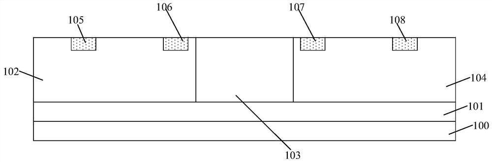
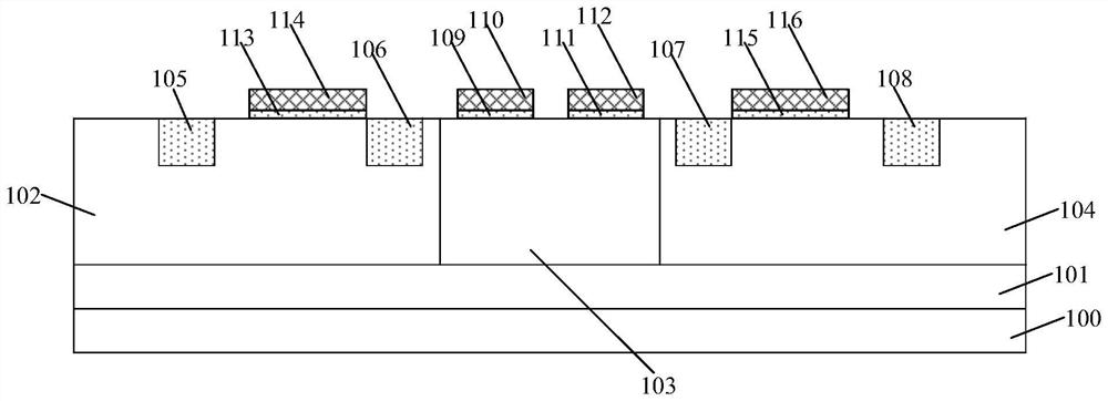
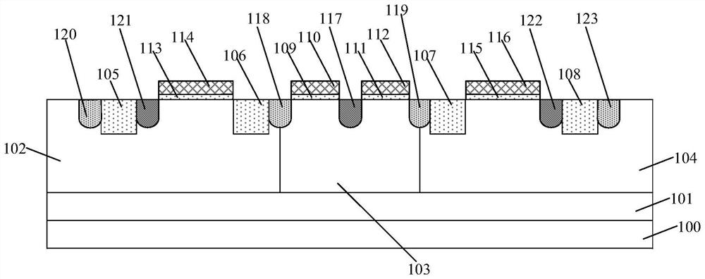
[0032] Figure 1 to Figure 4 It is a schematic cross-sectional structure diagram of the formation process of the electrostatic protection structure in the embodiment of the present invention.

[0033] Please refer to figure 1 , provide a substrate, the substrate has a well region, the well region includes adjacent first region 102, second region 103 and third region 104, the second region 103 is located between the first region 102 and the second region 104 Among the three regions 104 , the first region 102 and the third region 104 have the same conductivity type, and the first region 102 and the second region 103 have opposite conductivity types.

[0034] The conductivity type of the first region 102 includes N type or P type; the conductivity type of the second region 103 includes N type or P type; the conductivity type of the third region 104 includes N type or P type.

[0035] In this embodiment, the conductivity types of the first region 102 and the third region 104 inc...


PUM


Abstract

The invention discloses an electrostatic protection structure and a forming method thereof, and the structure comprises a substrate which is internally provided with a well region, and the well region comprises a first region, a second region and a third region which are adjacent to each other; the first gate structure and the second gate structure are located on the surface of the second region; the first doped region is located in the second region, and the first doped region, the first gate structure and the second gate structure are electrically connected; the second doped region stretches across the second region and the first region; the third doped region stretches across the second region and the third region, and the third doped region and the first doped region are located on the two sides of the second gate structure respectively; the fourth doped region and the fifth doped region are located in the first region, and the fourth doped region is electrically connected with the fifth doped region; the sixth doped region and the seventh doped region are located in the third region, and the sixth doped region is electrically connected with the seventh doped region. The performance of the electrostatic protection structure is improved.

Description

technical field [0001] The invention relates to the field of electrostatic protection devices, in particular to an electrostatic protection structure and a method for forming the electrostatic protection structure. Background technique [0002] In the process of human life and manufacturing, there is a phenomenon of charge accumulation and release every moment, which is called static electricity. Especially at the moment of charge release, its action time is short and the instantaneous current is large, which is extremely harmful to industrial manufacturing, especially the advanced integrated circuit industry. With the advancement of integrated circuits to advanced technology, the thickness of the gate oxide layer is reduced to the nanometer level, which is easily damaged in the process of electrostatic discharge. [0003] Conventional electrostatic discharge (ESD) protection devices, such as GGNMOS and GDPMOS, have low robustness. In order to achieve a higher electrostatic...

Claims


Application Information

Patent Timeline
Patent Type & Authority Applications(China)
IPC IPC(8): H01L27/02
CPCH01L27/0262
Inventor 范炜盛
Owner HUA HONG SEMICON WUXI LTD
Why Eureka
Try Eureka