Quantum dot light-emitting diode, preparation method thereof, display panel and display device

A quantum dot light-emitting and diode technology, which is applied in semiconductor/solid-state device manufacturing, electrical components, circuits, etc., can solve the problem of large difference in the number of holes and electrons

Active Publication Date: 2021-05-04
义乌清越光电科技有限公司 +1
View PDF7 Cites 0 Cited by
  • Summary
  • Abstract
  • Description
  • Claims
  • Application Information

AI Technical Summary

Problems solved by technology

[0004] Therefore, the technical problem to be solved by the present invention is to overcome the defect that the number of holes and electrons in the quantum dot light-emitting layer of the quantum dot light-emitting diode is greatly different, thereby providing a quantum dot light-emitting diode and its preparation method, display panel, and display device

Method used


Image

  • Quantum dot light-emitting diode, preparation method thereof, display panel and display device
  • Quantum dot light-emitting diode, preparation method thereof, display panel and display device
  • Quantum dot light-emitting diode, preparation method thereof, display panel and display device

Examples


Embodiment 1

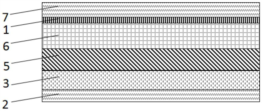
[0044] see figure 1 , the present embodiment provides a quantum dot light-emitting diode, comprising:

[0045] Quantum dot luminescent layer 5;

[0046] An electronic functional layer 6 located on one side of the quantum dot luminescent layer 5;

[0047] a cathode layer 7 located on the side of the electronic functional layer 6 away from the quantum dot light-emitting layer 5;

[0048] The passivation layer 1 located between the electronic function layer 6 and the cathode layer 7 , the passivation layer 1 includes several passivation portions at intervals.

[0049] In the above-mentioned quantum dot light-emitting diode, the passivation layer located between the electronic functional layer and the cathode layer includes several passivation parts at intervals, and the passivation part controls the interface between the electronic functional layer and the cathode layer. passivation, so that electrons can only be injected into the electronic functional layer through the gap be...

Embodiment 2

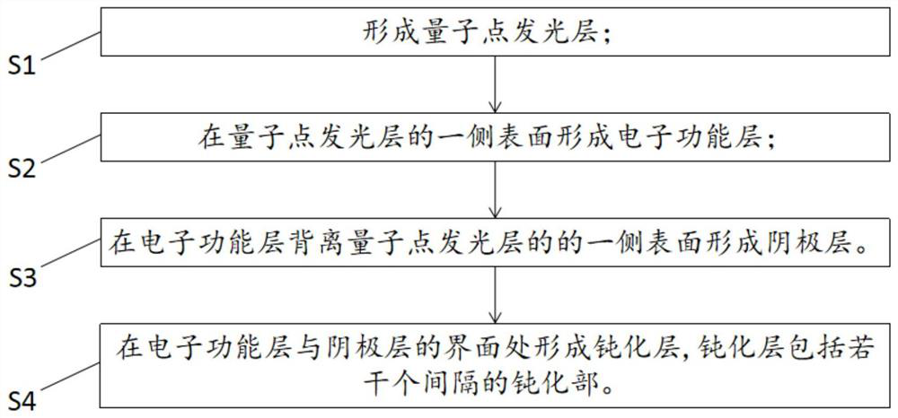
[0059] see image 3 , the present embodiment also provides a method for preparing a quantum dot light-emitting diode, comprising the following steps:

[0060] S1, forming a quantum dot light-emitting layer;

[0061] S2, forming an electronic functional layer on one side surface of the quantum dot light-emitting layer;

[0062] S3, forming a cathode layer on the surface of the electronic functional layer away from the quantum dot light-emitting layer;

[0063] S4. Form a passivation layer at the interface between the electronic function layer and the cathode layer, and the passivation layer includes several passivation portions at intervals.

[0064] The preparation method of the above-mentioned quantum dot light-emitting diode, by forming a passivation layer at the interface between the electronic functional layer and the cathode layer, the passivation layer includes several passivation parts at intervals, and the passivation part is opposite to the electronic functional lay...

Embodiment 3

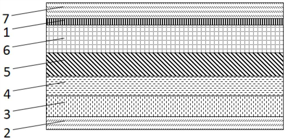
[0083] This embodiment provides a display panel, including: a substrate and the quantum dot light emitting diode provided in Embodiment 1, where the quantum dot light emitting diode is located on the substrate. A passivation layer is provided between the electronic functional layer and the cathode layer of the quantum dot light-emitting diode in the display panel, and the passivation layer includes several passivation parts at intervals. The interface of the cathode layer is passivated, so that electrons can only be injected into the electronic functional layer through the gap between the passivation parts, thereby reducing the injection efficiency of electrons into the electronic functional layer, and then reducing the transmission to the quantum dots. The difference in the number of holes and electrons in the light-emitting layer finally reduces the degree of electron accumulation in the quantum dot light-emitting layer and improves device performance.


PUM

PropertyMeasurementUnit
thicknessaaaaaaaaaa
energy densityaaaaaaaaaa

Abstract

The invention discloses a quantum dot light-emitting diode, a preparation method thereof, a display panel and a display device. The quantum dot light-emitting diode comprises a quantum dot light-emitting layer, an electronic function layer, a cathode layer and a passivation layer, wherein the electronic function layer is located on one side of the quantum dot light-emitting layer; the cathode layer is positioned on one side, deviating from the quantum dot light-emitting layer, of the electronic functional layer; and the passivation layer is positioned between the electronic function layer and the cathode layer, and comprises a plurality of passivation parts which are arranged at intervals. According to the quantum dot light-emitting diode, the number difference of holes and electrons transmitted to the quantum dot light-emitting layer is reduced, the electron accumulation degree in the quantum dot light-emitting layer is finally reduced, and the device performance is improved.

Description

technical field [0001] The invention relates to the technical field of display devices, in particular to a quantum dot light-emitting diode and a preparation method thereof, a display panel, and a display device. Background technique [0002] Quantum dot light-emitting diodes (QLEDs) have the advantages of high color purity, good stability, long life, good color temperature, and simple manufacturing process. They have great application prospects in the fields of next-generation flat panel displays and solid-state lighting. [0003] However, because the mobility of the electron transport layer is higher than that of the hole transport layer, the difference in the number of holes and electrons in the quantum dot light-emitting layer is large, and excess electrons accumulate in the quantum dot light-emitting layer, resulting in luminescence quenching, which is extremely The ground affects the luminous efficiency of the device. Contents of the invention [0004] Therefore, th...

Claims


Application Information

Patent Timeline
Patent Type & Authority Applications(China)
IPC IPC(8): H01L51/50H01L51/54H01L51/56H01L27/32
CPCH10K59/10H10K50/115H10K50/18H10K2102/00H10K71/00
Inventor 马中生穆欣炬刘高鹏刘航
Owner 义乌清越光电科技有限公司
Why Eureka
Try Eureka