Collector back side structure of insulated gate type bipolar transistor

A bipolar transistor and insulated gate technology, applied in circuits, electrical components, semiconductor devices, etc., can solve the problems of reducing the effective injection of back collector holes, unfavorable device conduction voltage drop, and reducing the efficiency of back injection, etc., to achieve The effect of reducing the risk of debris, reducing injection efficiency, and improving switching performance

Active Publication Date: 2013-04-24
JIANGSU CAS JUNSHINE TECH +1
View PDF5 Cites 1 Cited by
  • Summary
  • Abstract
  • Description
  • Claims
  • Application Information

AI Technical Summary

Problems solved by technology

[0008] In the patent US 2005/0227461, although it is mentioned that different methods are used to form P+/P- distribution, the injection efficiency of the back is reduced by this method, s

Method used


Image

  • Collector back side structure of insulated gate type bipolar transistor
  • Collector back side structure of insulated gate type bipolar transistor
  • Collector back side structure of insulated gate type bipolar transistor

Examples


Embodiment 1

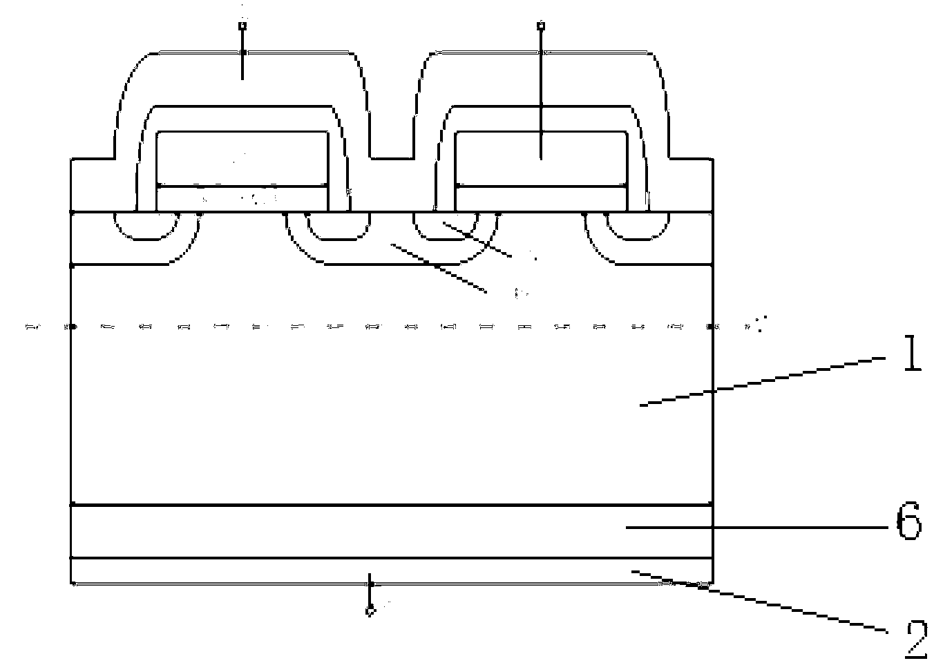
[0020] A collector back structure of an insulated gate bipolar transistor, which includes a silicon substrate layer 1 and a collector metal layer 2, and has high-concentration implantation regions 3 and low-concentration implantation regions 4 distributed at intervals on the backside of the silicon substrate layer 1 , and the thickness of the silicon substrate layer 1 corresponding to the high-concentration implantation region 3 is smaller than the thickness of the silicon substrate layer 1 corresponding to the low-concentration implantation region 4 .

[0021] Such as figure 2 As shown, depending on the structure of the front side, the back side is etched and forms different implant distributions. For the right under the implantation of the front P+ region, it is slightly thinner than other places by etching, and the thickness is determined according to the actual situation. For the lower part of the JFET area, no treatment is performed or the epitaxy method is used to make...

Embodiment 2

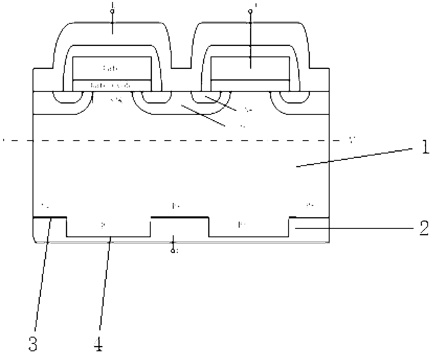
[0023] A collector back structure of an insulated gate bipolar transistor, which includes a silicon substrate layer 1 and a collector metal layer 2, and has high-concentration implantation regions 3 and low-concentration implantation regions 4 distributed at intervals on the backside of the silicon substrate layer 1 , and the thickness of the silicon substrate layer 1 corresponding to the high-concentration implantation region 3 is smaller than the thickness of the silicon substrate layer 1 corresponding to the low-concentration implantation region 4, and a buffer layer 5 is provided between the silicon substrate layer 1 and the collector metal layer 2 .

[0024] For the collector back structure of PT-type IGBT and the collector back structure of FS-type IGBT, such as image 3 shown.

Embodiment 3

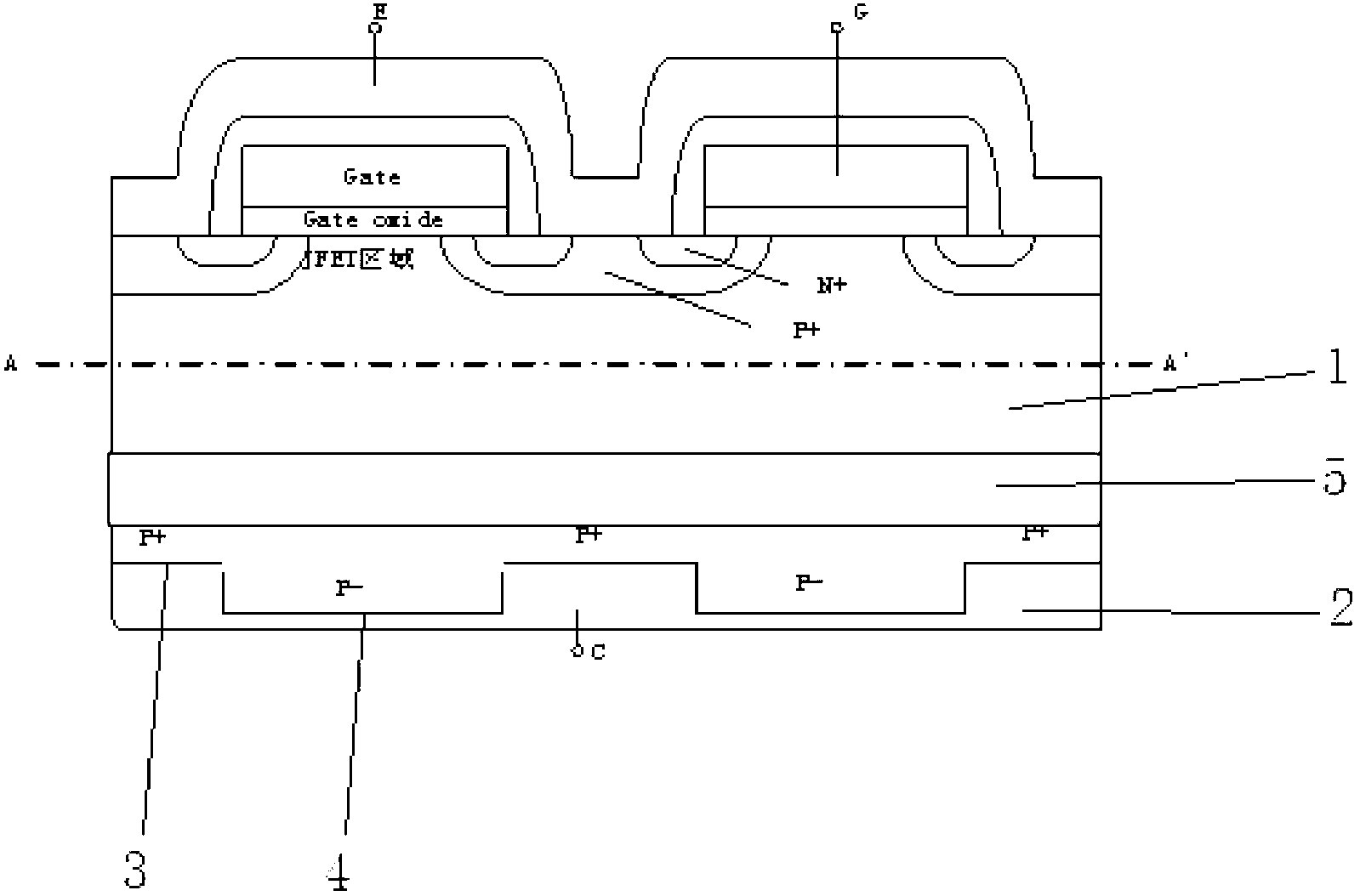
[0026] A collector back structure of an insulated gate bipolar transistor, which includes a silicon substrate layer 1 and a collector metal layer 2, and has high-concentration implantation regions 3 and low-concentration implantation regions 4 distributed at intervals on the backside of the silicon substrate layer 1 , and the thickness of the silicon substrate layer 1 corresponding to the high-concentration implantation region 3 is smaller than the thickness of the silicon substrate layer 1 corresponding to the low-concentration implantation region 4 .

[0027] For the back structure of the collector of the IGBT whose front is a trench type structure, such as Figure 4 shown.


PUM


Abstract

The invention relates to a collector back side structure of an insulated gate type bipolar transistor. The collector back side structure of the insulated gate type bipolar transistor comprises a silicon base layer and a collector metal layer, a high concentration injection region and a low concentration injection region distributed in a spaced mode are arranged on the back side of the silicon base layer, and thickness of the silicon base layer at the corresponding position of the high concentration injection region is smaller than thickness of the silicon base layer at the corresponding position of the low concentration injection region. By distributing the high concentration injection region and the low concentration injection region in a spaced mode, injection efficiency of the back side collector can be effectively reduced, and switch property of components is improved. Compared with sheet and ultrathin sheet process, average thickness of chips is increased and fractional danger can be reduced.

Description

technical field [0001] The invention belongs to the technical field of voltage-controlled power devices, and in particular relates to a collector back structure of an insulated gate bipolar transistor. Background technique [0002] IGBT: The acronym for Insulated Gate Bipolar Transistor, a voltage-controlled power device that is widely used as a high-voltage switch. Usually, according to the depletion of the electric field in the drift region, it is divided into PT-IGBT and NPT-IGBT. listed. [0003] In ordinary IGBTs, the thickness of each part of the chip is the same, and the back collector is usually only formed by P-type (such as B) implantation, and then activated by low-temperature annealing to form a P+ layer with uniform concentration. In the present invention, according to the different carrier mechanisms, the back is etched, and at the same time, the back is implanted unevenly to make P+ / P- interval distribution, so as to improve the dynamic and static performanc...

Claims


Application Information

Patent Timeline
IPC IPC(8): H01L29/739H01L29/08
Inventor 陈宏朱阳军吴凯徐承福卢烁今邱颖斌
Owner JIANGSU CAS JUNSHINE TECH
Why Eureka
Try Eureka