LED epitaxial structure and preparation method thereof

An epitaxial structure and structure layer technology, applied in electrical components, circuits, semiconductor devices, etc., can solve the problems of reducing the injection efficiency and luminous efficiency of light-emitting diodes, high junction temperature of LED chips, lattice mismatch, etc., to reduce internal reflection. Loss, performance improvement, effect of reducing operating voltage

Pending Publication Date: 2022-02-08
XIAMEN SILAN ADVANCED COMPOUND SEMICON CO LTD
View PDF7 Cites 1 Cited by
  • Summary
  • Abstract
  • Description
  • Claims
  • Application Information

AI Technical Summary

Problems solved by technology

[0003] Long-term aging under high temperature and high current will lead to excessively high junction temperature of the LED chip. Due to the slight lattice mismatch between the epitaxial structure layers, a large number of structural defects such as dislocations will be formed on the interface bet

Method used


Image

  • LED epitaxial structure and preparation method thereof
  • LED epitaxial structure and preparation method thereof
  • LED epitaxial structure and preparation method thereof

Examples


Embodiment 1

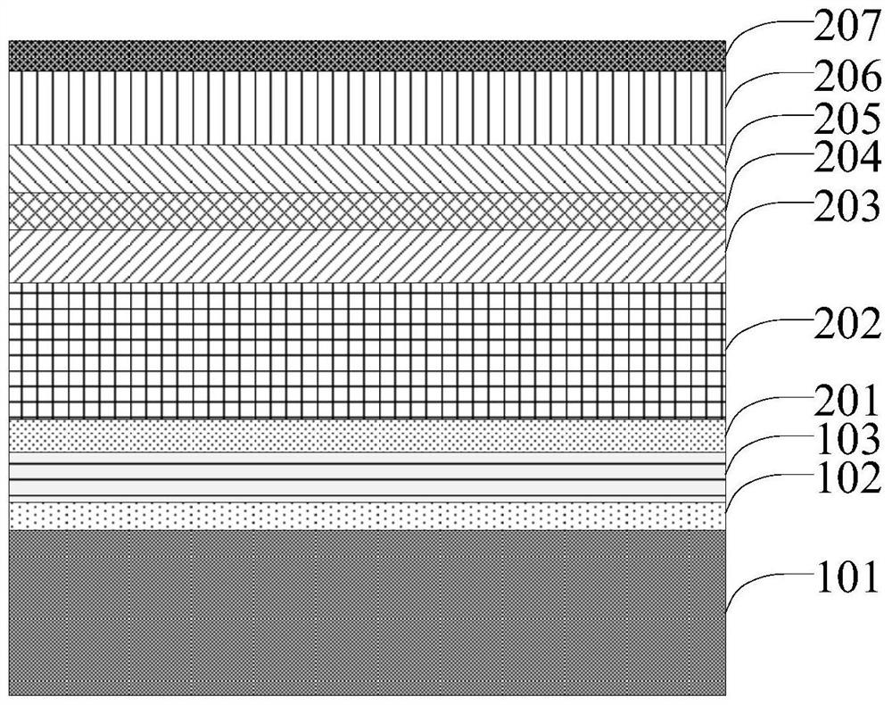
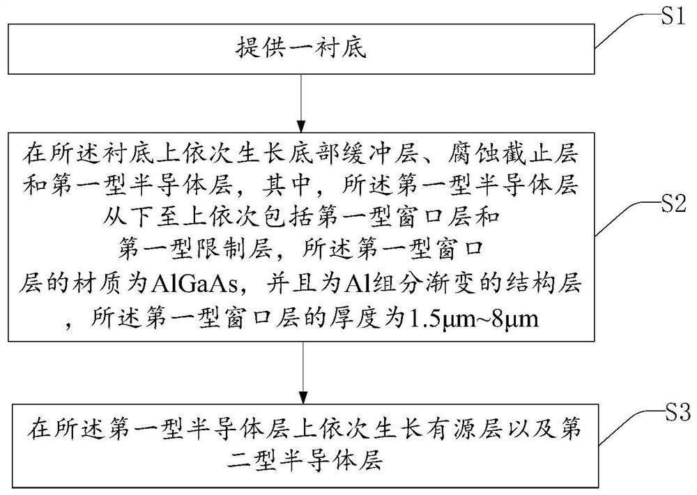
[0048] figure 1 It is a structural schematic diagram of the LED epitaxial structure of this embodiment. refer to figure 1 , the LED epitaxial structure includes from bottom to top: a bottom buffer layer 102 on the substrate 101, an etch stop layer 103, a first-type semiconductor layer, an active layer 204, and a second-type semiconductor layer, wherein the first The semiconductor layer includes a first-type window layer 202 and a first-type confinement layer 203 from bottom to top, and the first-type window layer 202 is a structural layer with a graded Al composition.

[0049] The first type semiconductor layer further includes a first type ohmic contact layer 201 , and the first type ohmic contact layer 201 is located between the etching stop layer 103 and the first type window layer 202 .

[0050] The second-type semiconductor layer includes, from bottom to top, a second-type confinement layer 205 , a second-type window layer 206 and a second-type ohmic contact layer 207 ....

Embodiment 2

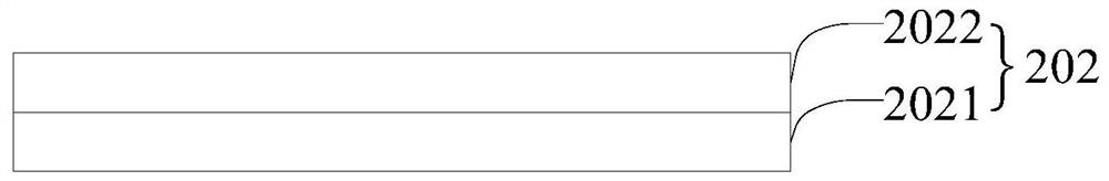
[0084] figure 2 It is a structural schematic diagram of the first type window layer of this embodiment. The difference between this embodiment and the first embodiment is only that the structure of the first-type window layer 202 is different, and the parts with the same structure will not be repeated here.

[0085] Specifically, the first-type window layer 202 in the LED epitaxial structure includes a two-layer structure composed of the first structure layer 2021 and the second structure layer 2022 or a structure composed of the first structure layer 2021 and the second structure layer 2022 stacked alternately. In the multi-period structure, the period number k ranges from 2 to 30, preferably 20-30. Such as figure 2 As shown, the first-type window layer 202 includes a two-layer structure composed of a first structural layer 2021 and a second structural layer 2022 . The material of the first structural layer 2021 is Al a Ga 1-a As, the material of the second structural ...


PUM

PropertyMeasurementUnit
Thicknessaaaaaaaaaa
Thicknessaaaaaaaaaa
Total thicknessaaaaaaaaaa

Abstract

The invention provides an LED epitaxial structure and a preparation method thereof. The LED epitaxial structure sequentially comprises a bottom buffer layer, a corrosion cut-off layer, a first type semiconductor layer, an active layer and a second type semiconductor layer from bottom to top, wherein the bottom buffer layer, the corrosion cut-off layer, the first type semiconductor layer, the active layer and the second type semiconductor layer are located on a substrate, the first type semiconductor layer sequentially comprises a first type window layer and a first type limiting layer from bottom to top, the first type window layer is made of AlGaAs and is a structural layer with an Al component being gradually changed, and the thickness of the first type window layer is 1.5 microns to 8 microns. The light emitting efficiency of the LED chip can be improved, the working voltage of the LED chip can be reduced and the high-temperature aging stability of the LED chip can be improved by forming the first type window layer with the Al component being gradually changed.

Description

technical field [0001] The invention relates to the technical field of semiconductors, in particular to an LED epitaxial structure and a preparation method thereof. Background technique [0002] Light Emitting Diode (LED, Light Emitting Diode) is a semiconductor solid light-emitting device, which has the advantages of simple structure, light weight, and no pollution. It has been widely used in many fields such as digital, display, lighting, and plant engineering. It is called environmental protection , Energy-saving green lighting source, contains huge business opportunities. Among them, the infrared light-emitting diode is an important light-emitting diode, which is widely used in remote control, vehicle sensing, closed-circuit television and other fields. The epitaxial structure of the infrared light-emitting diode is the basic structure for preparing the infrared light-emitting diode. [0003] Long-term aging under high temperature and high current will lead to excessive...

Claims


Application Information

Patent Timeline
IPC IPC(8): H01L33/30H01L33/12H01L33/14H01L33/00
CPCH01L33/30H01L33/12H01L33/14H01L33/0062
Inventor 廖寅生李森林毕京锋王亚宏
Owner XIAMEN SILAN ADVANCED COMPOUND SEMICON CO LTD
Why Eureka
Try Eureka