LED epitaxial structure and preparation method thereof

An epitaxial structure and structural layer technology, applied in electrical components, circuits, semiconductor devices, etc., can solve the problems of reducing luminous efficiency and affecting the light output efficiency of LED chips, and achieve the effect of improving light output efficiency, reducing internal reflection loss and improving performance.

Active Publication Date: 2021-12-21
XIAMEN SILAN ADVANCED COMPOUND SEMICON CO LTD
View PDF7 Cites 5 Cited by
  • Summary
  • Abstract
  • Description
  • Claims
  • Application Information

AI Technical Summary

Problems solved by technology

At present, a considerable part of the light generated in the active layer of AlGaInP-based LEDs will be confined in the device and cannot be completely coupled out, which will affect the light extraction efficiency of the LED chip and cause its luminous efficiency to decrease.

Method used


Image

  • LED epitaxial structure and preparation method thereof
  • LED epitaxial structure and preparation method thereof

Examples


preparation example Construction

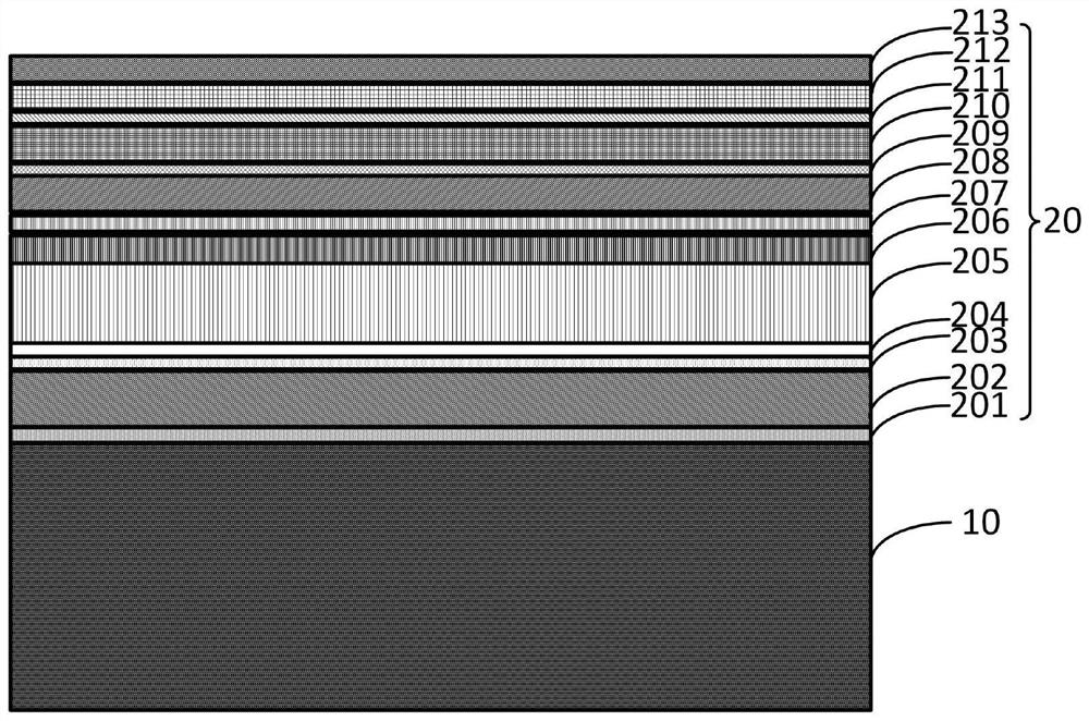
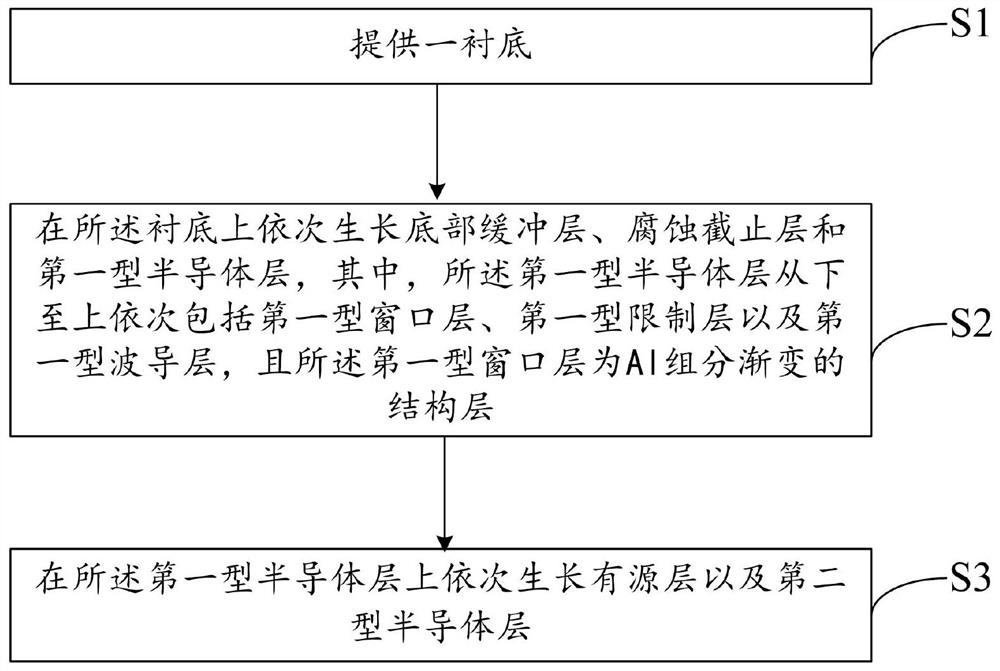
[0043] refer to figure 2 , the preparation method of the LED epitaxial structure 20 specifically includes the following steps:

[0044] Step S1: providing a substrate 10;

[0045] Step S2: growing a bottom buffer layer 201, an etch stop layer 202, and a first-type semiconductor layer sequentially on the substrate 10, wherein the first-type semiconductor layer includes a first-type window layer 205, a first-type semiconductor layer from bottom to top A type-1 confinement layer 206 and a first-type waveguide layer 207, and the first-type window layer 205 is a structural layer with a graded Al composition;

[0046] Step S3: growing an active layer 208 and a second type semiconductor layer sequentially on the first type semiconductor layer.


PUM

PropertyMeasurementUnit
thicknessaaaaaaaaaa
thicknessaaaaaaaaaa
thicknessaaaaaaaaaa

Abstract

The invention provides an LED epitaxial structure and a preparation method thereof. The LED epitaxial structure sequentially comprises a bottom buffer layer, a corrosion cut-off layer, a first type semiconductor layer, an active layer and a second type semiconductor layer from the bottom to the top, wherein the first type semiconductor layer sequentially comprises a first type window layer, a first type limiting layer and a first type waveguide layer from bottom to top, and the first type window layer is a structural layer with gradually-changed Al components. By forming the first type window layer with the gradually changed Al component, the light emitting efficiency of the LED can be improved, and the working voltage of the LED can be reduced.

Description

technical field [0001] The invention relates to the technical field of semiconductors, in particular to an LED epitaxial structure and a preparation method thereof. Background technique [0002] Light Emitting Diode (LED, Light Emitting Diode) is a semiconductor solid light-emitting device, which has the advantages of simple structure, light weight, and no pollution. It has been widely used in automotive lighting, decorative lighting, military lighting, communications, printing and other fields. The above-mentioned series of advantages of LED chips are called environmental protection and energy-saving green lighting sources, and they contain huge business opportunities. Among them, the III-V compound semiconductors represented by gallium arsenide (GaAs) have great applications in optoelectronic fields such as high-brightness light-emitting diodes and lasers due to their high luminous efficiency, high electron saturation drift speed, and stable chemical properties. potential...

Claims


Application Information

Patent Timeline
Patent Type & Authority Applications(China)
IPC IPC(8): H01L33/10H01L33/12H01L33/06H01L33/30H01L33/00
CPCH01L33/10H01L33/12H01L33/06H01L33/30H01L33/0062
Inventor 薛龙李森林杨美佳毕京锋
Owner XIAMEN SILAN ADVANCED COMPOUND SEMICON CO LTD
Why Eureka
Try Eureka