GaN-based LED integrated chip with multiple light-emitting sub areas

A technology of integrated chips and photons, applied in the direction of electrical components, electrical solid devices, circuits, etc., can solve the problems of PN junction short circuit, easy disconnection of interconnection lines, complicated process, etc., to prevent breaking, avoid small round corner bending, Enhance the effect of side wall reflections

Inactive Publication Date: 2014-04-16
南京大学扬州光电研究院
View PDF8 Cites 13 Cited by
  • Summary
  • Abstract
  • Description
  • Claims
  • Application Information

AI Technical Summary

Problems solved by technology

Although the above three methods can solve the problem that the interconnection line is easy to break or short-circuit the PN junction on the side wall of the light-emitting sub-region, they all have the disadvantage of complicated process.

Method used


Image

  • GaN-based LED integrated chip with multiple light-emitting sub areas
  • GaN-based LED integrated chip with multiple light-emitting sub areas
  • GaN-based LED integrated chip with multiple light-emitting sub areas

Examples


Embodiment 1

[0022] For front-mount LED chips that emit light from the p-GaN layer, the implementation steps are as follows:

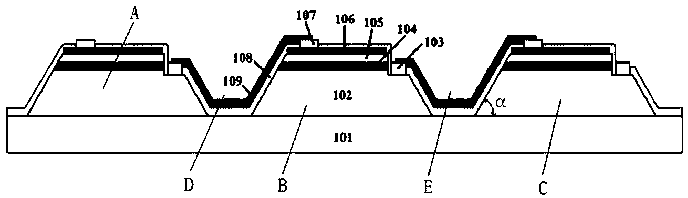
[0023] Step 1, take an LED epitaxial wafer, the specific structure includes a substrate 101, an epitaxially grown n-GaN layer 102, a quantum well active region 104, and a p-GaN layer 105, and form side walls by photolithography and dry etching The isolation trench is inclined at a large angle, the depth of the trench reaches the insulating substrate, and the included angle α between the side wall of the trench and the plane of the substrate is 30-80°. For the specific method, please refer to the content disclosed in the Chinese patent application with application number 201210492636.3.

[0024] In step 2, photolithography and dry etching are used to etch n-GaN steps in each light-emitting sub-region.

[0025] In step 3, a layer of ITO is evaporated on the entire chip as the current spreading layer 106, and then corresponding patterns are obtained by photolithograp...

Embodiment 2

[0034] For flip-chip LED chips that emit light from the substrate, the implementation steps are as follows:

[0035] Step 1, take an LED epitaxial wafer, the specific structure includes a substrate 101, an epitaxially grown n-GaN layer 102, a quantum well active region 104, and a p-GaN layer 105, and form side walls by photolithography and dry etching The isolation trench is inclined at a large angle, and the depth of the trench reaches the insulating substrate. Concrete method is identical with embodiment 1.

[0036] In step 2, photolithography and dry etching are used to etch n-GaN steps in each light-emitting sub-region.

[0037] In step 3, a reflective current spreading layer 106 is prepared on the surface of the p-GaN layer by photolithography, metal evaporation and Lift-off process, and the current spreading layer is also a mirror.

[0038] Step 4, deposit a layer of SiO on the whole wafer 2 As the insulating protective layer 108, part of SiO is etched by photolithogr...


PUM


Abstract

The invention discloses a GaN-based LED integrated chip with multiple light-emitting sub areas, and belongs to the technical field of LED chip structures. The GaN-based LED integrated chip with the multiple light-emitting sub areas comprises a substrate, an n-GaN layer, a quantum well active area, a p-GaN layer, a current spreading layer, a P electrode and at least two light-emitting sub areas. Grooves which are mutually isolated are formed between adjacent light-emitting sub areas, and the bottoms of the grooves are placed on the surface of the substrate. According to the GaN-based LED integrated chip with the multiple light-emitting sub areas, the open circuit probability is lowered to the maximum degree when an interconnecting wire stretches across the grooves, the emergent probability of internal total reflected light of the chip can be improved, internal reflection loss is reduced, and therefore light extraction efficiency is improved.

Description

technical field [0001] The invention belongs to the technical field of LED chip structure, and specifically relates to the technical field of monolithic integrated LED chip production. Background technique [0002] At present, the new generation of solid-state lighting sources represented by GaN-based LEDs have been gradually used in traffic lights, LCD backlights, street lights, Automobile lights, interior lighting, etc. [0003] In recent years, due to the shortcomings of traditional low-voltage, high-current-driven DC LED chips, such as complex drive circuit structure, large heat generation, low efficiency, and low reliability, according to different classifications of the circuit connection methods of the light-emitting sub-regions Methods, high voltage LED (High Voltage LED, referred to as HV-LED) chips and AC LED (Alternating Current LED, referred to as AC-LED) chips driven by high voltage and low current have gradually become an important content of research and deve...

Claims


Application Information

Patent Timeline
Patent Type & Authority Applications(China)
IPC IPC(8): H01L27/15H01L33/48H01L33/62
Inventor 徐洲陈鹏谭崇斌徐兆青张琳吴真龙徐峰高峰邵勇王栾井宋雪云
Owner 南京大学扬州光电研究院
Why Eureka
Try Eureka